ASIA ELECTRONICS INDUSTRYYOUR WINDOW TO SMART MANUFACTURING
imec, AT&S Zero in on Advanced IC Packaging
During the recent International Microwave Symposium, imec and AT&S presented a major step towards realizing a novel system integration approach. Hence, enabling integration of D-Band chips and waveguides into low-cost, mass-manufacturable PCBs.
This new approach paves the way for the development of compact, cost-effective, and high-performance 140 GHz (automotive) radar and 6G mobile communications systems. For that reason, offering significantly lower signal loss in comparison to planar PCB lines or substrate-integrated waveguides (SIWs) in PCBs and interposers.
Integrated Approach
The need for higher bandwidths in applications such as automotive radar and upcoming 6G mobile networks is fueling the demand for higher radio frequencies. Thus, the D-Band, spanning from 110 to 170 GHz, garners significant attention.
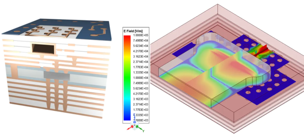
However, tapping into these frequencies poses challenges, such as increased system complexity and signal attenuation. Hollow air-filled substrate-integrated waveguide (AFSIW) technology with fully metalized sidewalls offers significantly reduced signal loss compared to substrate-integrated waveguides (SIWs) that use rows of vias and the planar interconnect technology used in current communication and radar systems. Despite this intrinsic benefit, a mass-production approach for PCBs with integrated AFSIW waveguides is currently unavailable.
“To facilitate the next generation of cost-effective, high-performance radar and communication systems, millimeter-wave front-end systems that can operate at frequencies exceeding 100 GHz are necessary. However, a key concern is how these antennas and millimeter-wave ICs can be optimally connected. We believe a key part of the solution is to utilize AFSIW technology. Unfortunately, such waveguides are expensive and hard to integrate into multi-layer PCBs or interposers,” said Ilja Ocket, program manager at imec.
For that reason, Ocket said Imec and AT&S have partnered to address this challenge. “Together, we demonstrate an integrated front-end combining imec’s 140 GHz radar ICs in combination with a novel packaging/module concept developed by AT&S. The demonstration of PCB-integrated AFSIWs is an important breakthrough towards achieving this end goal.”
Suits 140GHz Radar, 6G
As part of an advanced system module concept, AT&S and imec have collaborated to develop D-Band AFSIWs with solid copper sidewalls integrated into a multi-layer PCB to prevent signal leakage and to form arbitrarily shaped air cavities. It is the first successful demonstration of an AFSIW operating above 100 GHz, and integrated into a low-cost, mass-manufacturable PCB. By eliminating dielectric losses, so that only conductor losses remain, the new approach achieves a loss of 0.07 to 0.08dB/mm across the 115 to 155 GHz frequency range, translating into a five-fold reduction compared to reported planar PCB lines or SIWs in PCBs and interposers. These impressive results only represent a first step, as further improvements will continue to drive down losses even further in the coming years.
“Imec’s 140 GHz radar chips and packaging design expertise have given us a significant head start. We believe that our new packaging approach can be utilized to create efficient, compact, and high-resolution 140 GHz radar modules for automotive applications, creating vehicles that are increasingly ‘aware’ of what is happening, both in-cabin and around them,” said Erich Schlaffer, program manager R&D Electronics Solution at AT&S. “Additionally, this technology will find its way in 6G mobile networks.”
- Share: