ASIA ELECTRONICS INDUSTRYYOUR WINDOW TO SMART MANUFACTURING
Toshiba to Boost Power IC Grit With New 300mm Fab
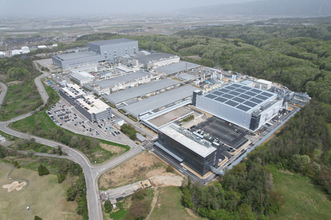
Toshiba Electronic Devices & Storage Corporation recently held a ceremony to mark the completion of a new 300mm wafer fab facility for power semiconductors. In addition, it also opened a new office building at Kaga Toshiba Electronics, both in Ishikawa Prefecture, Japan.
The completion of construction is a major milestone for Phase 1 of Toshiba’s multi-year investment program. Moreover, Toshiba will now proceed with equipment installation, toward starting mass production in the second half of fiscal year 2024.
Taps AI, Sophisticated Technologies
Once Phase 1 reaches full-scale operation, Toshiba’s production capacity for power semiconductors, mainly MOSFETs[1] and IGBTs[2], will be 2.5 times that of fiscal 2021[3]. Decisions on the construction and start of operation of Phase 2 will reflect market trends.

The new manufacturing building follows and will majorly contribute to Toshiba’s Business Continuity Plan (BCP). Furthermore, it has a seismic isolation structure that absorbs earthquake shock and redundant power sources.
Meanwhile, the facility will employ energy from renewable sources and solar panels on the roof of the building (onsite PPA model). Thus, allowing the facility to meet 100% of its power requirement with renewable energy.
Most importantly, Toshiba will employ artificial intelligence (AI) to boost product quality and production efficiency.
Toshiba expects to receive a grant from the Ministry of Economy, Trade and Industry of Japan to subsidize its investment in part of the manufacturing equipment.
Expects Robust Growth of Automation
Power semiconductors play a crucial role in electricity supply and control. Thus, are essential devices for energy efficiency in all electrical equipment. With the continuing electrification of automobiles and the automation of industrial machinery, the company expects continued robust demand growth.
Toshiba started power semiconductor production on a new 300mm wafer line in the second half of fiscal 2022 at Kaga Toshiba Electronics’ existing facility. Going forward, the company will expand production with the new fab and further contribute to carbon neutrality.
Notes:
[1] Metal-Oxide-Semiconductor Field-Effect Transistor
[2] Insulated Gate Bipolar Transistor
[3] The total of 200- and 300-millimeter wafer fabrication capacity (200-millimeter equivalent)


