ASIA ELECTRONICS INDUSTRYYOUR WINDOW TO SMART MANUFACTURING
Canon Ships NIL System to TIE, Spurs New Chip R&D
Canon Inc. ships its most advanced lithography platform, the FPA-1200NZ2C nanoimprint lithography (NIL) system for semiconductor manufacturing, to the Texas Institute for Electronics (TIE), a Texas-based semiconductor consortium.
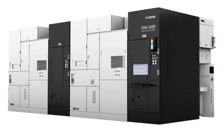

Basically, Canon became the first in the world to commercialize a semiconductor manufacturing system that uses NIL technology. It was during the FPA-1200NZ2C’s release on October 13, 2023. Particularly, the NIL technology forms circuit patterns differently from conventional projection exposure technology.
Mainly, the conventional photolithography equipment transfers a circuit pattern by projecting it onto the resist coated wafer. On the contrary, the new product does it by pressing a mask imprinted with the circuit pattern into the resist on the wafer like a stamp. Because its circuit pattern transfer process does not go through an optical mechanism, fine circuit patterns on the mask can be faithfully reproduced on the wafer. With reduced power consumption and cost, the new system enables patterning with a minimum linewidth of 14nm1. This is equivalent to the 5nm node2 required to produce most advanced logic semiconductors currently available.
This FPA-1200NZ2C will be used at TIE for the research and development of advanced semiconductors and production of prototypes.
Meanwhile, TIE is a semiconductor consortium founded in 2021 and is supported by The University of Texas at Austin. It consists of state and local governments, semiconductor companies, national research institutions and other entities. Primarily, TIE provides open access to semiconductor research and development initiatives and prototyping facilities to help solve issues related to advanced semiconductor technology, including advanced packaging technology.
Generally, Canon will continue to promote research and development using nanoimprint lithography systems for semiconductor manufacturing to contribute to the evolution of semiconductor manufacturing technology.
1 Nanometer- one billionth of a meter
2 nm node – refers to a generation of technology in the semiconductor manufacturing process
-26 September 2024-
- Share: