ASIA ELECTRONICS INDUSTRYYOUR WINDOW TO SMART MANUFACTURING
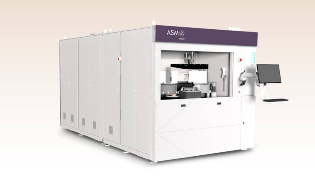
ASM to Boost SiC Grit with New PE2O8 Line
At the 2024 International Conference on Silicon Carbide and Related Materials, ASM International N.V. introduced the PE2O8 silicon carbide epitaxy system. Specifically, it is a new, dual chamber, platform for silicon carbide (SiC) epitaxy (Epi). Designed to address the needs of the advanced SiC power device segment, the PE2O8 is the benchmark epitaxy system for low defectivity. Moreover, it also conforms high process uniformity all with higher throughput and low cost of ownership needed to enable broader adoption of SiC devices.
Recently, the general electrification trend drives more power device manufacturers to utilize SiC for a growing number of high-power applications. Among them are for electric vehicles, green power, and advanced data centers. Thus, the expanded demand and requirements for lower cost for SiC is causing a transition from 6” to 8” SiC substrates.
At the same time, SiC device manufacturers are designing higher power devices that will benefit from better SiC epitaxy.
Utilizing a unique design, the dual chamber PE2O8 system deposits SiC with ultra precise control. Therefore, enabling benchmark higher yield and higher throughput. The highly compact, dual chamber design enables high productivity and low total costs of operation.
In addition, the system features an easy preventive maintenance approach helping to increase uptime and reduce the occurrence of unscheduled downtime. System deliveries have been ongoing to multiple customers globally, among them leaders in SiC power device manufacturing.
Extended System Capability
“We are at a critical inflection for silicon carbide power products, as our customers transition from 6” to 8” wafers”, said Steven Reiter, Corporate Vice President, and business unit head of Plasma and Epi at ASM. Furthermore, Reiter said, “Delivering a high-quality epitaxy process on larger wafers with defectivity control is critical, and we have been the industry benchmark for process uniformity with our novel chamber design. We have now extended our system capability to improve our process control and our value for customers with lower cost of ownership.”
Since 2022, ASM, through its new SiC Epi product unit has been developing and refining its single wafer SiC epitaxy system. Moreover, with the structurally higher demand for electric vehicles and improvement of the overall SiC wafer and device yield, the equipment market for SiC epitaxy has grown substantially in recent years.
02 October 2024
- Share: