ASIA ELECTRONICS INDUSTRYYOUR WINDOW TO SMART MANUFACTURING
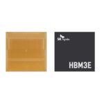
SK hynix Eyes New Platform for Future DRAM Tech
SK hynix Inc. has announced it is considering shifting to its latest technologies for its next generation DRAM technology. Specifically, the company took note of the scaling challenges for its sub-10nm technologies.
Cha Seon Yong, Chief Technology Officer of SK hynix, delivered a speech in one of the plenary sessions at the IEEE VLSI symposium 2025 in Kyoto, Japan. In his speech, Cha took note of the increasingly difficult to improve performance and capacity of scaling through teh current technology platform.
“In order to overcome such limitations, SK hynix will apply the 4F² VG (Vertical Gate) platform and 3D DRAM technology to technologies of 10-nanometer level or below with innovation in structure, material and components,” he said.

What is 4F² VG Platform?
The 4F² VGplatform is a next-generation memory technology that minimizes the cell area of DRAM. Moreover, it enables high-integration, high-speed and low-power through a vertical gate structure.
4F² is the area occupied by one cell, a unit to store data indicated as F² where F is the minimum feature size of a semiconductor. Therefore, 4F² is an integration technology to put more cells in a chip, wherein one cell occupies an area of 2F by 2F.

Meanwhile, VG, or the vertical gate, is a structure similar to a gate. It acts as a switch of a transistor and is vertically placed and surrounded by channels. Currently, it is a flat structure where a gate is laid horizontally on top of channels.
Currently, 6F2 cells are common, but by applying 4F2 cell and wafer bonding technology that puts the circuit part below the cell area, cell efficiency and electrical characteristics can be improved.
3D DRAM Roadmap
At the same time, Cha also introduced 3D DRAM as the main pillar for the future DRAM along with VG.
Moreover, Cha said that although some in the industry warn of cost increase according to the number of layers stacked, it can be solved by constant technological innovation.
Along with structural breakthrough, the company will also strive to find a new growth engine by sophisticating technologies of critical materials and components of DRAM to lay foundation for the next 30 years.
“Until around 2010, DRAM technology was expected to face limitations at 20 nanometers, but with constant innovation, we have made it this far,” said Cha.
In addiiton, Cha said, “SK hynix will continue to guide the future of long-term technological innovation to be a milestone for young engineers in the field of DRAM and maintain cooperation within the industry to bring future of DRAM into reality.”
10 June 2025
- Share: