ASIA ELECTRONICS INDUSTRYYOUR WINDOW TO SMART MANUFACTURING
Applied Unveils New Chipmaking Tools for Angstrom-Era
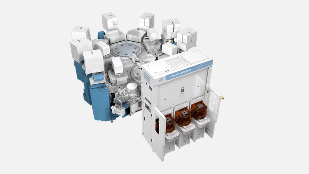
Applied Materials is pushing deposition innovation as a key enabler for the angstrom era of chipmaking. Specifically, the company introduced two new systems designed to help customers scale Gate-All-Around (GAA) transistors at 2nm-class nodes and beyond.
The company says the platforms deliver atomic-level control over critical films where process tolerances can approach the size of individual atoms—an increasingly decisive factor as AI-driven designs pack more functionality into tighter footprints.
Inevitable for AI-Era Logic
As foundries move from FinFETs to GAA, they face a sharp rise in integration complexity. Applied points to advanced logic flows that can exceed 500 process steps, with many requiring repeatable deposition of metals and dielectrics across high-aspect-ratio features and tight within-wafer control. The company also highlights the scale of AI-era logic: next-generation GPUs under development may integrate more than 300 billion transistors in an area roughly the size of a postage stamp, raising the cost of leakage, parasitics, and variability at the device and system levels.
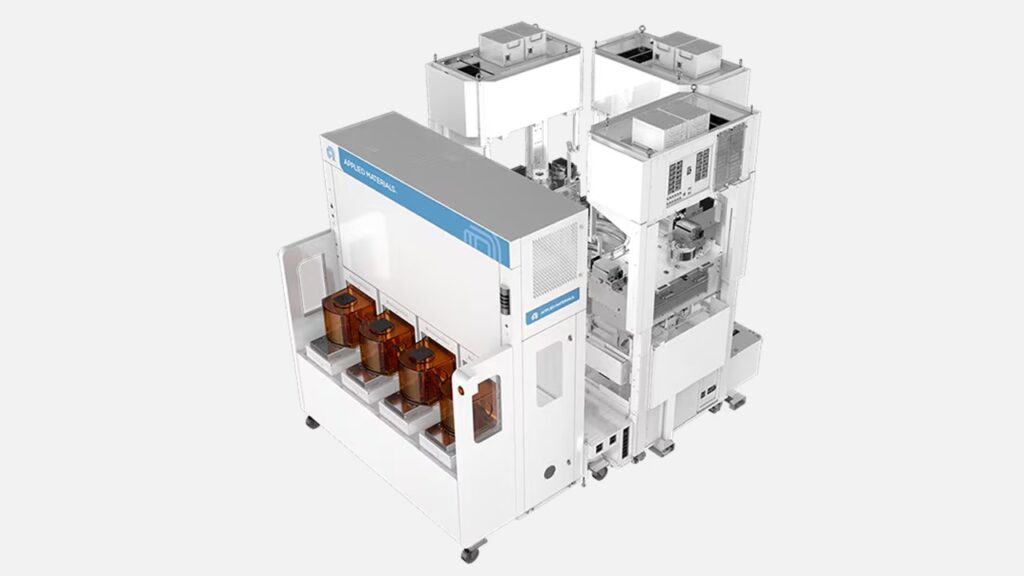
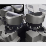
The first new platform, Applied’s Precision Selective Nitride PECVD system, is designed to form selective silicon nitride films that the company says can help protect shallow trench isolation (STI) structures at advanced logic nodes. In the release, Applied links STI integrity to scaling outcomes such as reduced parasitic capacitance and better device performance and power. The company positions the selective nitride approach as a way to maintain electrical isolation as transistor density rises and integration flows become more demanding.
The second system, Trillium ALD, targets GAA metal gate-stack formation, where increasingly thin, conformal layers must coat complex 3D structures with minimal variation. Applied says Trillium enables advanced metal gate stacks for nanosheet transistors and provides tighter control over ultrathin films that influence threshold voltage. In the company’s framing, that kind of atomic-scale repeatability becomes essential as device dimensions shrink into the angstrom era and variability directly impacts yield and product power targets.
Essential Materials for Advanced Chips
Dr. Prabu Raja, President of the Semiconductor Products Group at Applied Materials, said the industry is entering a period of rapid, non-linear change. Thus, traditional chip scaling alone is no longer sufficient.
“At the most advanced angstrom-class logic nodes, performance and power are increasingly determined by materials. Thanks to our foundational leadership in materials engineering, these deposition systems will enable our customers to deliver critical transistor inflections that are foundational to the AI computing roadmap,” said Raja.
Applied also said leading foundry-logic manufacturers are already using the new deposition systems for 2nm-class development and beyond—an indicator that deposition control and materials selectivity are now treated as frontline requirements for GAA scaling programs.
For process integration and device engineers, Applied’s message is that the deposition steps surrounding isolation and gate-stack formation are becoming more sensitive—and more influential—at 2nm-class nodes. By emphasizing selective nitride for STI-related structures and ALD control for advanced metal gate stacks, the company is pointing to a practical path for managing parasitics and threshold-voltage variation as GAA architectures mature. In short, Applied is arguing that materials engineering inside deposition tools is increasingly where advanced-node power and performance margins are won or lost.
10 April 2026
- Share: