ASIA ELECTRONICS INDUSTRYYOUR WINDOW TO SMART MANUFACTURING
Applied Materials to Soar AI Chips with New Systems
Applied Materials has introduced a portfolio of semiconductor manufacturing systems aimed at enabling advanced three-dimensional (3D) chip architectures that support next-generation artificial intelligence (AI) workloads. The move addresses rising constraints in computing performance driven by the growing gap between processing power and memory capabilities.
As AI models expand, data movement and memory bandwidth have become critical bottlenecks across computing systems. This “memory wall” is accelerating the adoption of advanced packaging technologies such as high-bandwidth memory (HBM) and 3D stacking, which offer significant improvements in efficiency and speed but increase production complexity.
Epitaxy Innovation Enhances DRAM Performance
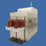
One of the key advancements is an enhanced version of Applied’s Centura Prime Epi system. The upgraded solution applies selective growth of doped materials to improve transistor performance in DRAM. By combining precise doping with advanced strain engineering, the system boosts drive current and energy efficiency, helping meet the demands of HBM and next-generation memory standards.
“The transistor and materials technologies that drove performance gains in leading-edge logic are now becoming essential in DRAM,” said Dr. Prabu Raja, President of the Semiconductor Products Group at Applied Materials. “By leveraging our epitaxy leadership, Applied is uniquely positioned to drive this transition.”
The new system also features a reduced footprint, allowing chipmakers to scale production capacity more efficiently within fabrication facilities.
Advanced Packaging Systems Improve Yield, Precision
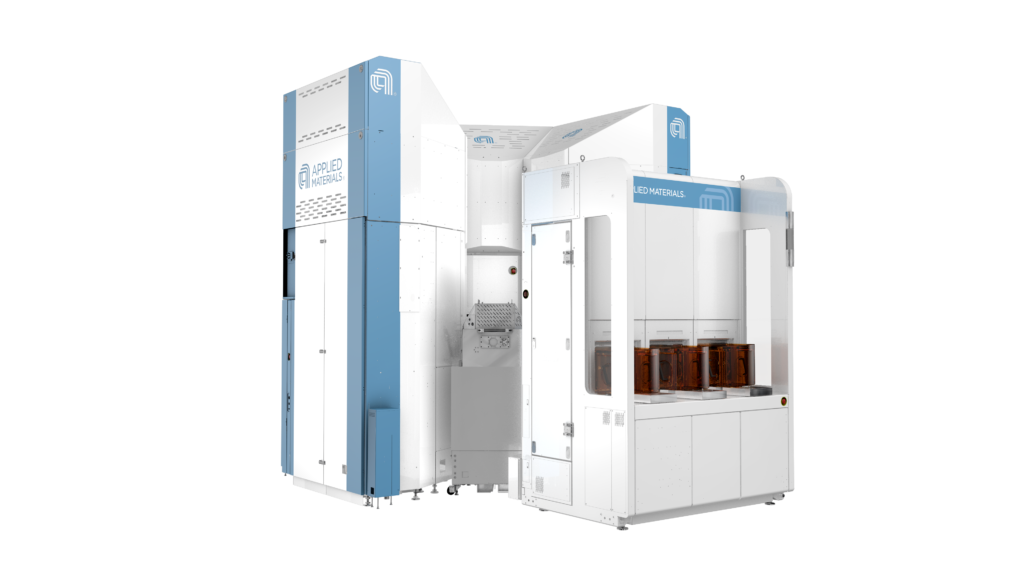
Applied Materials also introduced three new systems targeting critical steps in advanced packaging. These include a chemical mechanical planarization (CMP) platform designed to enhance wafer uniformity, an electrochemical deposition system that improves copper interconnect consistency, and a deposition system that strengthens ultra-thin chip layers for reliable stacking.
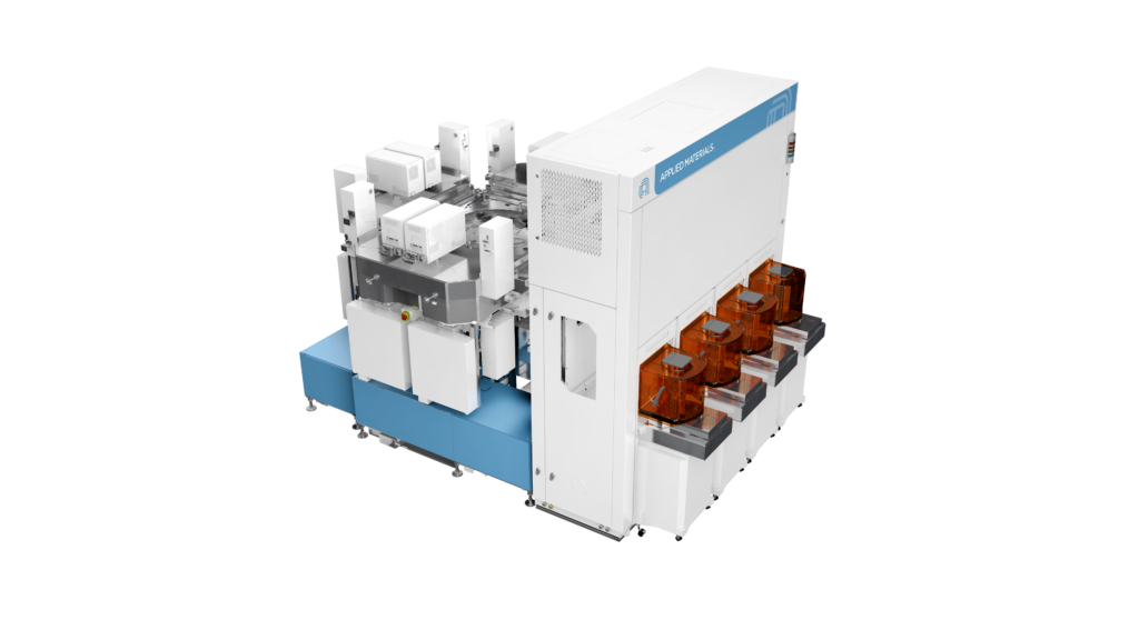
The Opta Quad CMP is engineered specifically for advanced packaging, where thicker films, longer polish times and tighter tolerances raise the risk of non-uniformity and yield loss. Opta Quad continuously monitors wafer conditions during polish and dynamically adjusts in real time, improving within-wafer uniformity and total thickness variation control.
The Nokota Vmax 2 ECD is an electrochemical deposition (ECD) system engineered for high-precision copper plating across a broad range of applications for next-generation packaging, from TSV fill for 3D stacking to fine-pitch interconnects such as microbump formation. In essence, the Nokota Vmax 2 helps ensure the TSVs and microbumps are leveled across the entire wafer, which is critical because as 3D stacks scale, uneven interconnects can leave gaps that prevent reliable contact between layers.
Meanwhile, Producer Avila 2 is a plasma-enhanced chemical vapor deposition (PECVD) system that improves the mechanical stability of ultra-thin DRAM dies by depositing stress-balanced dielectric films around TSVs, enabling reliable stacking of 12, 16, and future high-layer-count HBM designs.
These innovations are designed to support hybrid bonding and other emerging 3D integration technologies, where precision is critical to ensure performance and manufacturing yield.
Supporting the Future of AI Computing
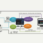
To address defect detection challenges in advanced packaging, Applied unveiled two new electron beam (eBeam) systems for metrology and defect review. These tools provide sub-10nm measurement sensitivity and high-resolution defect classification across complex substrates, improving yield management in high-volume production environments.
With its expanded portfolio, Applied Materials is positioning itself at the center of the evolving semiconductor landscape. By integrating innovations across materials engineering, packaging, and process control, the company aims to help chipmakers accelerate production of high-performance, energy-efficient AI chips.
28 June 2026
- Share: