ASIA ELECTRONICS INDUSTRYYOUR WINDOW TO SMART MANUFACTURING
IBM Unveils Breakthrough 0.7nm Chip Tech
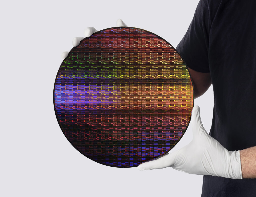
IBM has announced a major advancement in semiconductor design with the debut of a sub-1 nanometer chip built on a 0.7 nm (7 angstrom) process. The development signals a breakthrough for an industry approaching the physical limits of conventional chip scaling.
The new chip integrates nearly 100 billion transistors into a footprint roughly the size of a fingernail—almost double the density of IBM’s 2 nm technology introduced in 2021. The innovation is designed to support growing computational demands across artificial intelligence (AI), cloud infrastructure, and next-generation devices.
Nanostack Architecture Enables Performance Gains
At the core of the new chip is IBM’s “nanostack” architecture, a three-dimensional transistor design that stacks nanosheet components vertically. This approach goes beyond traditional nanosheet technology, enabling more efficient use of space while enhancing flexibility in material selection for each layer.
The architecture introduces a new method of building chips by stacking and staggering transistors, allowing engineers to optimize performance and power efficiency independently at each level. According to IBM, the chip can deliver up to 50 percent higher performance or achieve up to 70 percent greater energy efficiency compared to its 2 nm counterpart.
Designed for Next-Generation Workloads
The sub-1 nm technology is expected to significantly enhance compute-intensive applications such as generative AI and high-bandwidth data processing. IBM also reported improvements in memory scaling, with research indicating a 40 percent reduction in SRAM footprint, enabling more efficient chip designs.
The breakthrough has been validated through multiple technical demonstrations, including successful CMOS integration, dual-channel engineering, and functional circuit operation, confirming the design’s viability for real-world computing.

Extending the Semiconductor Roadmap
IBM’s innovation highlights a pathway for continued miniaturization in chipmaking, even as features approach atomic dimensions. The company projects that the nanostack design could support at least a decade of scaling advancements.
The work is being developed in collaboration with industry partners at a semiconductor research facility in Albany, New York. IBM is also progressing efforts in advanced lithography and quantum computing, including plans for a dedicated quantum foundry.
IBM expects early adoption of the new sub-1 nm technology within the next five years, positioning it as a foundation for future computing systems.
26 June 2026
- Share: