ASIA ELECTRONICS INDUSTRYYOUR WINDOW TO SMART MANUFACTURING
Canon Releases New Stepper Option for 3D Chip Packaging
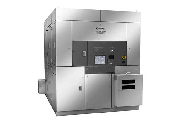
Canon Inc. launches in Japan the FPA-5520iV LF2 Option for back-end process semiconductor lithography i-line stepper system that contributes to 3D advanced packaging technologies. It highlights 0.8µm resolution and a wide exposure field of 100×100 mm. Specifically, a stepper is semiconductor lithography system that utilizes a 365nm wavelength mercury lamp as the light source.
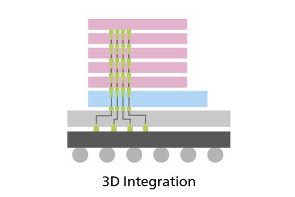
In the field of semiconductor chip performance enhancement, higher-density packaging in back-end processes attracts greater attention. This trend runs alongside miniaturization of circuits in front-end process of semiconductor manufacturing. Advanced packaging, which realizes high performance, requires fine rewiring. In recent years, semiconductor lithography systems have been used for this purpose. There is a growing need for increasing semiconductor performance through 2.5D technology1. In 2.5D semiconductor chips are integrated with extremely high die-to-die interconnect density. Moreover, the demand for 3D technology2, in which active chips are integrated by die stacking for the shortest interconnect and smallest package footprint, is also high.
High Resolution in Wide Exposure
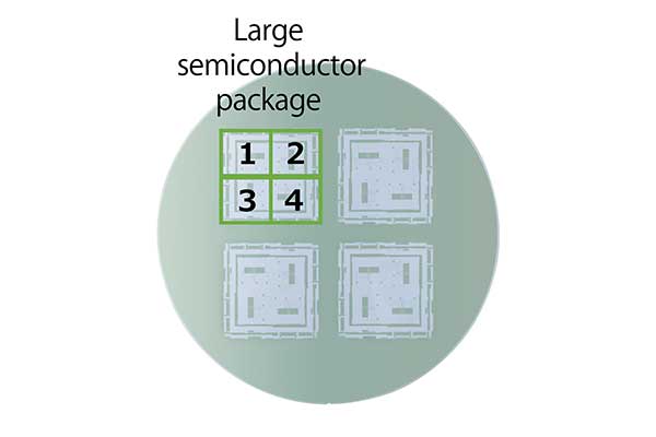
The new FPA-5520iV LF2 Option highlights a high resolution of 0.8µm. It also features 4-shot exposure with minimal distortion to make possible a wide exposure field of 100×100mm. This enables mass production of large and dense packaging with circuit patterns that integrate 2.5D and 3D technologies.
Additionally, the FPA-5520iV LF2 Option reduces distortion aberration of less than 1/4 that of its predecessor model, the FPA-5520iV LF Option (released in April 2021). The new model also features a new projection optical system with greater light level uniformity. These advancements allow LF2 Option steppers to provide 0.8µm resolution across a large 52×68mm single-exposure field. At the same time, it makes possible an ultra-wide 100×100mm exposure field.
Moreover, the FPA-5520iV LF2 Option inherits the basic performance of the FPA-5520iV, which can handle warped reconstituted substrates. This is an issue that can occur in packaging layers during mass-production process. Also, it delivers the same high productivity to enhance availability by detecting alignment marks—even on the reconstituted substrates3 with large chip array variations.
Going forward, Canon will strive to support further technological innovation by expanding its lineup of semiconductor lithography system offerings not only for front-end semiconductor chip manufacturing processes, but also systems that support state-of-the-art back-end packaging technologies.
Notes:
1Packaging to combine different chips. The chips can be placed close together and connected electrically by a number of circuits to increase processing capability.
2Refers to Through Silicon Via (TSV) technology, where memory chips are stacked to achieve high capacity.
3Wafers created by attaching and encasing in resin multiple individual semiconductor chips that are produced during the front-end processes of semiconductor manufacturing.
- Share: