ASIA ELECTRONICS INDUSTRYYOUR WINDOW TO SMART MANUFACTURING
New Technology Lifts Japan Superiority in IC Process
It has been quite some time the industry has been hearing digital transformation (DX). Larger capacity data can create new applications, such as digital twin, augmented reality (AR), virtual reality (VR), and even metaverse.
These have been previously difficult to achieve because of accuracy concerns and response speed.
The semiconductor market supports such society. However, amid the investment competition, many Japanese companies lost their share in the semiconductor market. With the expansion of DX applications, challenges between energy consumption and decarbonization have started to emerge. This clears the way for Japanese companies with new photonics-electronics convergence technology as a game changer in manufacturing process.
Challenges in Infrastructure
In the DX era, all related applications conform to high-speed data transmission, real-time representation at remote locations, and sharing of data among multiple points. However, present technologies have challenges, such as reproduction accuracies in the cyber space.
For example, digital twin can reproduce the behavior of a machine, but it cannot express behaviors of components inside its machine. Therefore, in remote equipment operation management, data accuracy is coarse, and cannot identify the essential problem. To overcome these challenges, using fifth-generation (5G) tele-communications and the higher-frequency tele-communications, enables even larger communication band, lower latency, and tele-communications among multiple locations.
Drastic Reduction of Power Consumption of Data Management Infrastructure
Relatedly, there is a need to also boost infrastructure (data centers) that store, analyze and feedback those data. As such, the use of greater amount of data necessitates data analysis not only at edges but also in the cloud.
The market of data centers that support cloud services, by hyperscale like Google, Amazon, Facebook, Apple, Microsoft (GAFAM) and so on, will definitely expand remarkably in the coming years. As they consume large amounts of electric power for cooling CPUs, the reduction of power consumption becomes more imminent than ever before to keep up with the market expansion in the future. Recent research shows data centers consume around 3 percent of global electricity use.
Companies have already taken decarbonization measures, such as energy savings, taking part in Renewable Energy 100% (RE100) global initiative, and the use of renewable energy. However, data centers require drastic reduction of power towards decarbonization. As one of the measures, there is a need to revisit computing and switching using electric wiring.
Use of Photoelectric Conversion Devices
Technologies as measures to solve the above-described issues are photoelectric conversion devices as well as optical transmission technology called all photonics network (APN). As such, it is possible to achieve higher-speed transmission and lower power consumption by changing conventional electric wiring.
These technologies have been developed in Japan since over 20 years ago. In 2019, NTT put to practical use a compact and low-power transistor using photonic crystal, increasing feasibility in one go. In addition, many Japanese companies have been engaged in IC peripheral technologies, such as co-packaged optics, as well as in the manufacture of transistors.
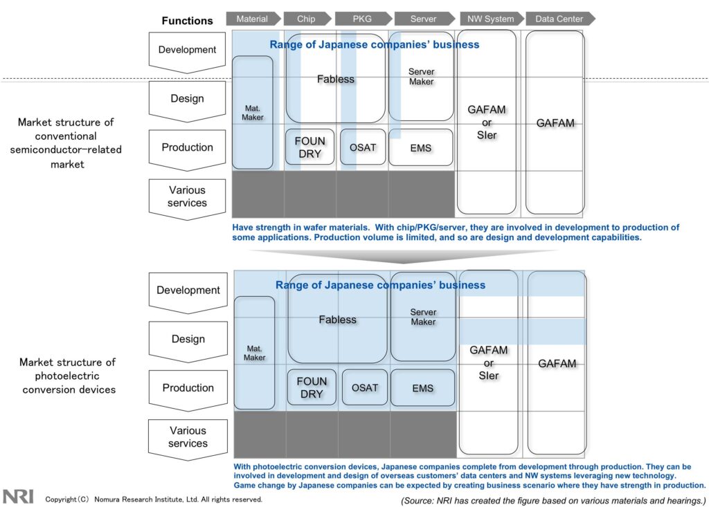
Supply chain from the front-end to back-end processes of photoelectric conversion devices manufacturing is available in Japan. Meanwhile, the back-end process, including packages, requires very high precision engineering design and manufacturing, such as the jointing of optical waveguides. This has been a barrier for late comers who enter this field.
Using Photoelectric Conversion Device Manufacturing of Japan
Japanese companies have been developing photonics-electronics convergence technology and possess mass production technology. As the adoption of DX becomes more dominant, introduction of photonics-electronics convergence technology is becoming more indispensable as well.
In the conventional semiconductor market, Japanese companies could not acquire sufficient manufacturing technology to complement standardization. However, with photonics-electronics convergence technology, Japanese companies possess differentiating manufacturing technologies.
For the first time in a while, Japanese companies have competitive advantages in photonics-electronics convergence technology for all semiconductor-related technologies. Japan’s semiconductor industry can establish superiority by creating new business model that leverages their advantages as manufacturing technology in addition to development (Fig. 1).
About This Article:
The author is Kenichi Sasaki, Senior Consultant, Consulting Division, Nomura Research Institute Co., Ltd. His field of specializations include:
・Devices and their applications (IoT products)
・MEMS/ Nano technology/ Sensors
・Factory IoT (manufacturing innovation)
・Data Center business etc.
- Share: