ASIA ELECTRONICS INDUSTRYYOUR WINDOW TO SMART MANUFACTURING
New X-Ray Techniques Improve Wafer Film Thickness
Wafer film is required to have ultra-thin thickness of up to several nanometers for advanced products. The accuracy of the film thickness greatly affects the quality of the semiconductor and therefore should be evaluated with a high-definition inspection device.
The film thickness is measured with X-rays in two ways. One is when X-ray is on a wafer, fluorescent X-rays with different wavelengths are exited depending on the atomic type constituting the material. The other is the film thickness calculated using the calibration curve between the intensity and the film thickness for these fluorescent X-rays, having energy inherent to each material.
Equipped With Two-Dimensional Detector
X-rays are emitted from X-ray tubes, but their intensity gradually deteriorates. Rigaku Corporation has the excellent technology that automatically performs proper corrections to keep accurate measurement with the use of software. The error can be reduced by numerically correcting the amount of incident X-ray absorbed by a film and that of the fluorescent X-ray.
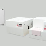
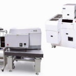
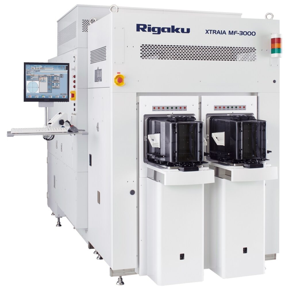
The X-ray film thickness and density monitor of XTRAIA MF-3000, the third generation of MFM310, is equipped with the two-dimensional detector HyPix-3000.
Approximately, 300,000 pixel sensors with a size of 100µm are configured in the detection unit in both vertical and horizontal directions. Each sensor has an amplifier and a circuit. When an X-ray photon is incident, each pixel sensor becomes conductive and therefore can count the number of incident photons one by one.
Using two-dimensional detector and X-ray reflectivity (XRR) measurement, the measurement speed of MF-3000 has been improved five times compared with the conventional model. In addition, XRR and X-ray diffraction (XRD) measurement have enabled the measurement of very thin and low crystallinity films, for which the demand is increasing.
Microcrystalline thin films with low crystallinity are being used in cutting-edge devices such as DRAM, magnetoresistive random access memory (MRAM), next-generation transistors, and 12 nanometer insulating films.
Develops Own Technologies
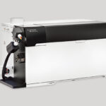
Another advantage Rigaku offers is its ability to develop elemental technologies by itself. HyPix-3000 is produced at the Yamanashi plant. A multi-layer mirror in which the incidence angle can be changed by controlling the film thickness is manufactured by a subsidiary in Michigan, United States. Because X-rays are not reflected by an optical mirror, they are collected and reflected by a multilayer film of 1,000 layers of molybdenum or silicon with properly adjusted film thickness.
This X-ray mirror is based on the unique technology of making a mirror surface with a curve at the angstrom level. The equipment for manufacturing such curved mirrors has also been developed by the company.
The X-ray module equipped with a multilayer mirror is sold as COLORS. It is used in semiconductor inspection equipment that uses X-rays and extreme ultraviolet (EUV) light, the demand for which is growing.
MFM310 has been shipped mainly for memory. From the third generation, it is also put into the market of logic semiconductors for much wider use in whole semiconductor manufacturing processes.
Memory cells have a relatively large area of several millimeters or more, but logic semiconductors have only a small and narrow space. A measurement pattern with 50 micrometer square on a scribe line should be irradiated, requiring a smaller beam spot (irradiation diameter).
With the conventional equipment, the diameter was limited to 35 micrometers. With the newly developed X-ray module “COLORS-t”, the irradiation diameter can be reduced to 20µm. The X-ray intensity generally becomes weaker as the irradiation diameter is reduced. However, the intensity has been improved by the processing technology and coating technology of the multilayer mirror.
- Share: