ASIA ELECTRONICS INDUSTRYYOUR WINDOW TO SMART MANUFACTURING
Impurity Analysis Plays Critical Role in IC Fab
Silicon wafer, which is the base material of semiconductors and the substrate for ICs, has an extremely high-purity single crystal structure. Because the concentration of contained impurities affects the quality of the product, the silicon needs to have the ultra-high purity of “Eleven Nine”. Eleven 9s means getting 99.999999999 percent or higher of ultra-high purity.
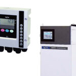
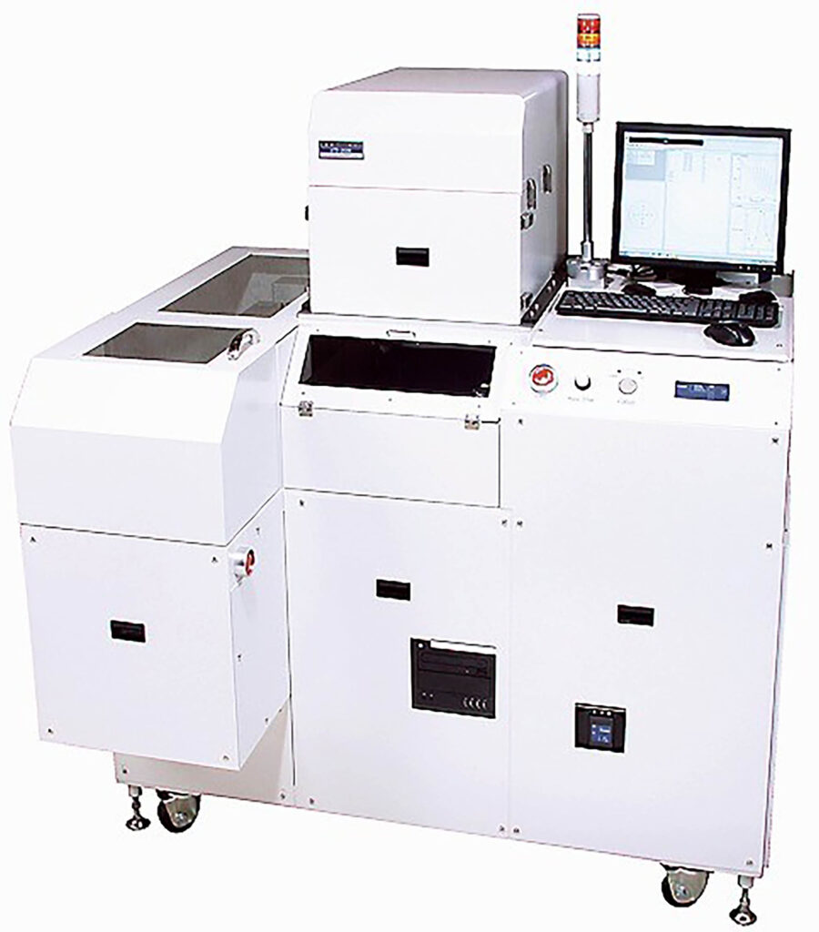
The Fourier Transform Infrared Spectrometer (FTIR) of JASCO Corporation irradiates a sample with infrared light and measures transmitted and reflected light. It can quantify trace amounts of impurities such as carbons and oxygens in silicon and analyze the mainstream 12-inch (about 30cm) wafers in the non-destructive and the non-contact manner.
High Purity in IC Fabs
Various regulations set the upper limit of the amount of contained impurities. The Japan Electronics and Information Technology Industries Association (JEITA) requires carbon components should be less than 40 billion atoms per cubic centimeter at room temperature.
Materials at room temperature constantly vibrate and generate thermal noise, which interferes with infrared measurements. Lower temperatures suppress the movement of the silicon crystal lattice.
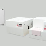
HCS-2000 uses a refrigerator to cool a sample to an extremely low temperature of 15K (-258°C). Liquid nitrogen or liquid helium does not require the cooling medium and carbon concentration could be up to 4ppba (4 billion per 1cm3).
There is also a great demand for measuring impurities in gas. Gas measurement using FTIR demonstrates infrared light passing through a cell with accumulated gas. As such, measures the concentration of the infrared absorption of the gas.
With the increase of the cell path length through which the gas flows, the measurable concentration becomes lower. On the other hand, a full vacuum type measures a very small amount of water molecules in the high-purity nitrogen gas and the like. By making the optical path in vacuum, the evaluation is possible without the influence of water in the atmosphere.
Targets Analysis Efficiency
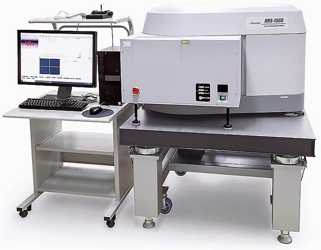
According to JASCO, due to the current trend of increasing production of semiconductors, inquiries are increasing for the measurement of carrier concentration using a laser Raman spectrophotometer. Measurement of free electron concentration is possible for n-type compound semiconductors, such as SiC and GaN containing carriers with a negative charge.
There are components caused by the Raman scattering, having a wavelength different from the incident light due to the excitation of molecular vibrations. Raman spectroscopy analyzes material structure at the molecular level using this weak scattered light.
The carrier concentration affects the lattice vibration of a crystal. If silicon has high crystallinity, it vibrates regularly. In laser Raman spectroscopy, measuring carrier concentration is possible by observing of the detailed form of the lattice vibration in the crystal.
Higher current can flow in the material with higher carrier concentration. However, materials with high carrier concentration are not necessarily the best. Semiconductor manufacturers utilize the laser Raman spectroscopy to find the optimum carrier concentration for the device application.
The company aims to improve efficiency of the analysis, enabling mapping (multipoint) measurement of the entire surface of the wafer using software specially made for measuring the concentration of carriers in SiC.
- Share: