ASIA ELECTRONICS INDUSTRYYOUR WINDOW TO SMART MANUFACTURING
ROHM Delivers Full Potential of GaN Devices
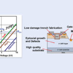
Gallium nitride (GaN) is a wide bandgap semiconductor, which has been attracting attention in the industry along with SiC (silicon carbide). Particularly, it is possible to reduce the on-resistance per unit area of GaN devices compared with Si. In addition, the chip size can be reduced for the same on-resistance, and the switching loss becomes much lower.
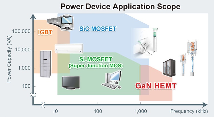
SiC devices are evolving toward higher withstand voltage and higher power. On the other hand, GaN devices are evolving toward higher frequency drives. For that reason, these devices have started to be used for different applications (see Figure 1).
For example, in applications such as for LiDAR, it is necessary to build a system that can acquire higher-definition images using narrow pulse signals. Therefore, GaN devices driven at high frequencies are most suitable and have started to be introduced in the market.
Overview of GNE10xxTB Series
The GNE10xxTB Series of GaN HEMTs, which has been lined up as the brand “EcoGaNTM” of ROHM Co. Ltd., contributes to energy saving and miniaturization. Furthermore, it has succeeded in the increase of the rated gate-source voltage from the conventional 6 V to higher 8 V using a unique structure (see Figure 2).
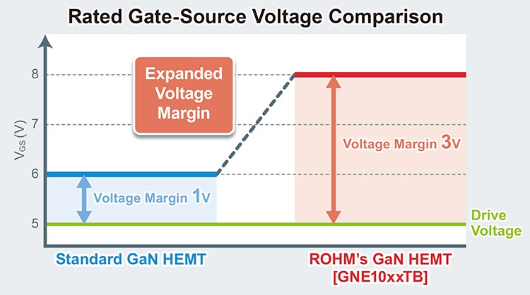
This increase ensures the device will not degrade even if the voltage overshoots 6V during switching. This contributes to the improvement of the design margin and reliability of the power supply circuit.
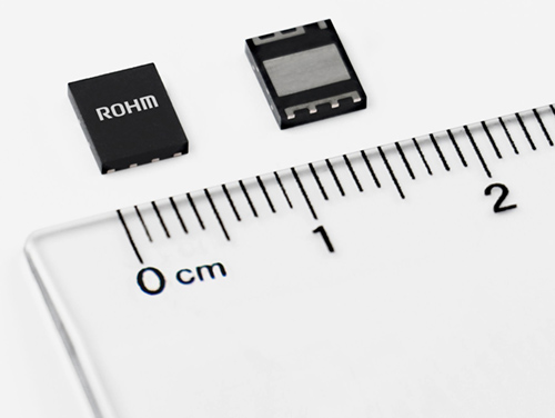
In addition, it has been commercialized in a highly versatile package that supports large currents and has excellent heat dissipation. Hence, this makes handling easy in the mounting process. Subsequently, the specific functions and effects of the GNE10xxTB series are available below.
Unique Structure Expands Rated Gate Source
A typical GaN HEMT with withstand voltage of 200V or less has a rated gate-source voltage of 6V for a gate drive voltage of 5 V due to its structure. This narrows the voltage margin to as small as 1V. Moreover, exceeding the rated voltage of the device may cause reliability problems such as deterioration and destruction. For that reason, the requirement of the highly accurate control of the gate drive voltage has been a major issue in the spread of GaN HEMTs.
A unique structure has been adopted in this product for the purpose of solving this issue. As a result, the rated gate-source voltage has successfully been increased from the conventional 6V to 8V. This stands as the industry’s highest as of December 2022. Furthermore, the device does not degrade even if overshoot voltage exceeds 6V during switching, contributing to higher reliability of the power supply circuit.
Excellent Heat Dissipation
This product uses a highly versatile package that supports large currents and has excellent heat dissipation. In addition, the reliability and the mountability of the package have been well established. Therefore, the product can be easily handled in the mounting process.
Furthermore, the package uses copper clip bonding technology. Thus, its parasitic inductance has been reduced by 55% compared to conventional products. For that reason, it is possible to maximize the performance of GaN HEMTs when designing circuits for high-frequency operation.
Solutions Maximizing Performance of GaN HEMTs
For the full use of the potential of GaN HEMTs that can be driven at a high speed, the gate driver IC must also operate at a high speed. Accordingly, the company has started providing samples of the 1-channel high-speed gate driver IC “BD2311NVX-C” for driving the GaN HEMT. The BD2311NVX-C supports a minimum input pulse width of 1.25ns (Typ.). The output delay of the driver with respect to input signal is extremely small, that is, 3.4 ns (turn-on) and 3.0 ns (turn-off).
This IC is ideal for driving GaN HEMTs because it can suppress the overshoot voltage to the gate with the unique control technology developed by the company. Furthermore, like EcoGaNTM, the adoption of a surface-mount package makes the product easy for board mounting.
The solution using GaN HEMTs and a gate driver IC for driving a GaN HEMT can drive laser diodes for LiDAR. Furthermore, its application is possible to DC-DC converters operating at high frequencies with the full use of the potential of GaN devices.
The converters are used in power supply circuits for various industrial equipment and IoT communication equipment such as base stations, data centers, etc.
Reference Design to Support Board Designing
The company has developed a reference design “REFLD002” for the LiDAR laser drive. This combines the GaN HEMT (EcoGaNTM), the gate driver IC for driving GaN HEMT, and a semiconductor laser diode device, and has released the design information (see Figure 3).
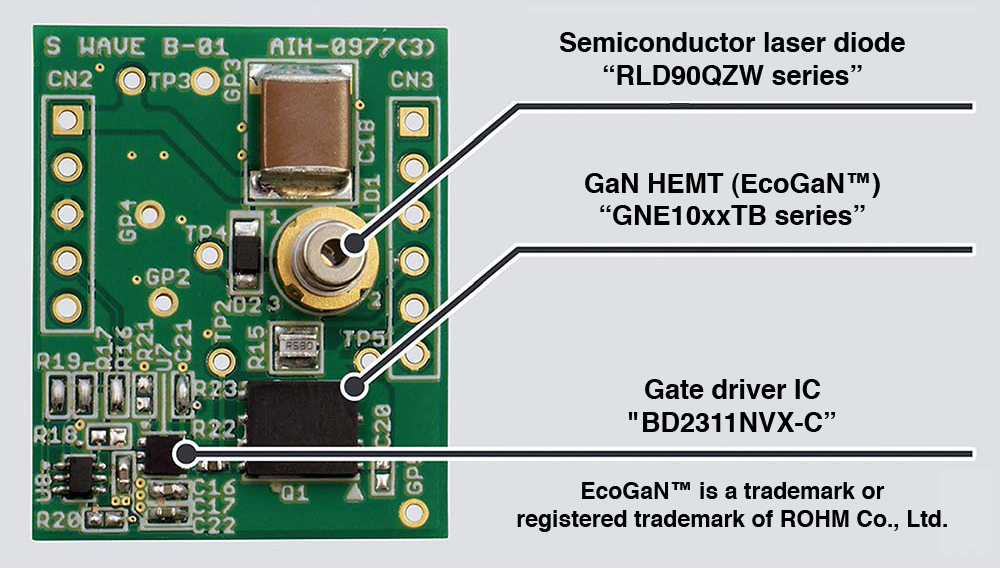
The applications of LiDAR are expanding not only for self-driving cars but also for industrial and infrastructure applications. Therefore, the provided reference design will contribute to the improvement of the performance of LiDAR (detection distance, resolution, etc.).
- Share:


About This Article:
ROHM Co. Ltd. provided the contents of this article.