ASIA ELECTRONICS INDUSTRYYOUR WINDOW TO SMART MANUFACTURING
Lam Research Study Points to Human-Machine Collaboration for Chip Innovation
In a new study, Lam Research Corp. examined the potential for the use of artificial intelligence (AI) in process development for chip fabrication today. It is a human-driven step that is essential for the mass production of every new advanced semiconductor in the world.
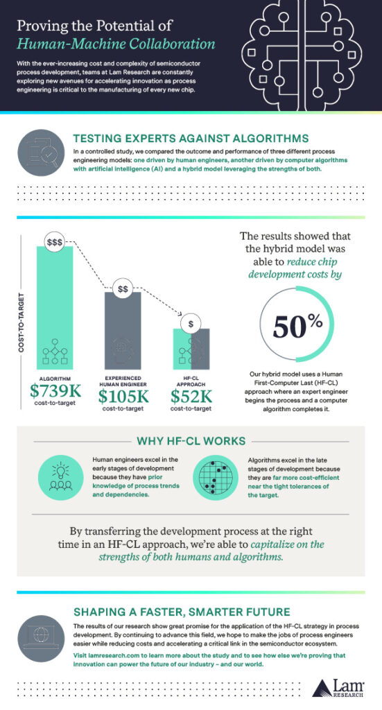
As the semiconductor market progresses towards $1 trillion in annual revenue by 20301, the study recently published in the journal Nature, identifies an opportunity to address two grand challenges facing the industry: reducing development costs and accelerating the pace of innovation to meet the increasing demand for next-generation chips. The study found that a “human-first, computer-last” approach can reach process engineering targets dramatically faster and at half the cost compared to today’s approach.
“New approaches in innovation are needed to enable the industry to scale fast enough to meet the data-driven world’s evolving demand for next-generation chips,” said Tim Archer, president and chief executive officer at Lam Research. “The opportunity for greater collaboration between talented engineers and machines in process engineering highlighted in Lam’s study in Nature is a potential game-changer for our customers and our industry at large. This research is a testament to Lam’s more than 40-year heritage of industry leadership and semiconductor manufacturing innovation. I congratulate the Lam team on this exciting work.”

Hybrid Human-First, Computer-Last Strategy
The rising complexity of next-generation chips continues to drive process development to be more challenging and expensive. Seeking a more efficient approach, researchers at Lam put talented process engineers head-to-head against AI-enabled computer algorithms in the study.
To manufacture every chip or transistor designed, experienced and skilled engineers must first create a specialized recipe that outlines the specific parameters and permutations needed for each process step. Hundreds of steps are required to build these nanometer-sized devices on a silicon wafer. Process steps typically include multiple instances of depositing thin layers of materials onto silicon wafers and etching away excess material with atomic-scale precision. This essential phase of semiconductor development is currently done by human engineers, largely using their intuition and a “trial and error” approach.
With every recipe unique to the chip design and more than 100 trillion possible options to incorporate, process development can be laborious, time-intensive, and costly. This increasingly slows down the time needed to achieve the next technology breakthrough.
In the Lam study, machine and human participants competed to create a targeted process development recipe at the lowest cost, weighing a variety of factors associated with test batches, metrology and overhead expenses. The study concluded that while humans excelled in solving challenging and out-of-the-box problems, a hybrid human-first, computer-last strategy can help address the tedious aspects of process development and, ultimately, speed up process engineering innovation.
“Although critical to the creation of each and every chip produced, the plasma physics of process engineering has been for decades rooted in the same scientific approach that Thomas Edison used: trial and error,” said Rick Gottscho, executive vice president and strategic advisor to the CEO – Innovation Ecosystem at Lam Research and co-author of the study.
“Our research showed that while engineering talent remains essential to innovation, process engineering costs can be reduced by 50 percent by integrating AI at the right stage and with the right data. The study provides a prescriptive approach for bringing together the best of human-led engineering and the best of what data science and machines offer to create a combination that performs better than either one alone. If realized, this hybrid approach can lead to significant savings in both dollars and engineering time for the industry,” said Gottscho.
Lam is currently incorporating the key learnings from the study into its development operations. The Lam study provides initial guidance on how to successfully integrate human knowledge, skill and experience with AI’s ability to rapidly assess numerous possible combinations in process engineering.
“By complementing engineering expertise with AI using the human-first, computer-last approach, the tedious and laborious aspects of design are alleviated for engineers, freeing them up to focus on the creative areas of development and explore innovations that may have been out of reach either due to bandwidth or cost,” said Keren Kanarik, technical managing director of Lam Research, lead author of the research paper and a former process engineer.
“While the application of AI in process engineering is still in its infancy and human expertise and domain knowledge is essential for the foreseeable future, the results point us to a path to foundationally change the way processes are developed for manufacturing chips.”
1- Source: McKinsey and Co., “The semiconductor decade: A trillion-dollar industry,” April 1, 2022


