ASIA ELECTRONICS INDUSTRYYOUR WINDOW TO SMART MANUFACTURING
Mitsubishi Electric Installs First 12-inch Wafer Processing Line
Mitsubishi Electric Corporation announced the completion of the installation of its first 12-inch silicon wafer processing line at its Power Device Work’s Fukuyama Factory. Specifically, the plant manufactures power semiconductors. Also, the power semiconductor chips processed on this production line achieved the required performance levels. This was verified through sample production and testing.
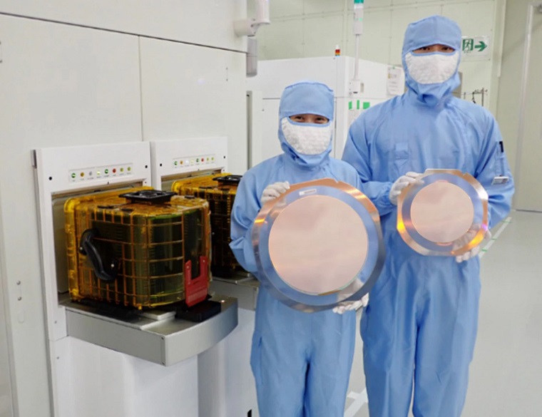
As previously announced, Mitsubishi Electric is planning to start mass production on the new 12-inch silicon wafer line in FY2025. The company aims to approximately double its silicon power semiconductor wafer processing capacity by FY2026 compared to FY2021 levels.
In recent years, the demand for power semiconductors offering efficient control of electrical power has grown as countries look to achieve carbon-free status. Power semiconductors are utilized in a wide range of relevant products. Among them include electric vehicles, consumer devices (e.g. air-conditioning systems), industrial equipment, renewable energy, and traction devices. Moreover, a stable supply is required to meet this growing demand.
Mitsubishi Electric will contribute to the realization of a carbon-free society through the enhancement of its production capacity. Also, it will ensure a stable supply of power semiconductors through the introduction of highly efficient 12-inch wafer production lines.
- Share: