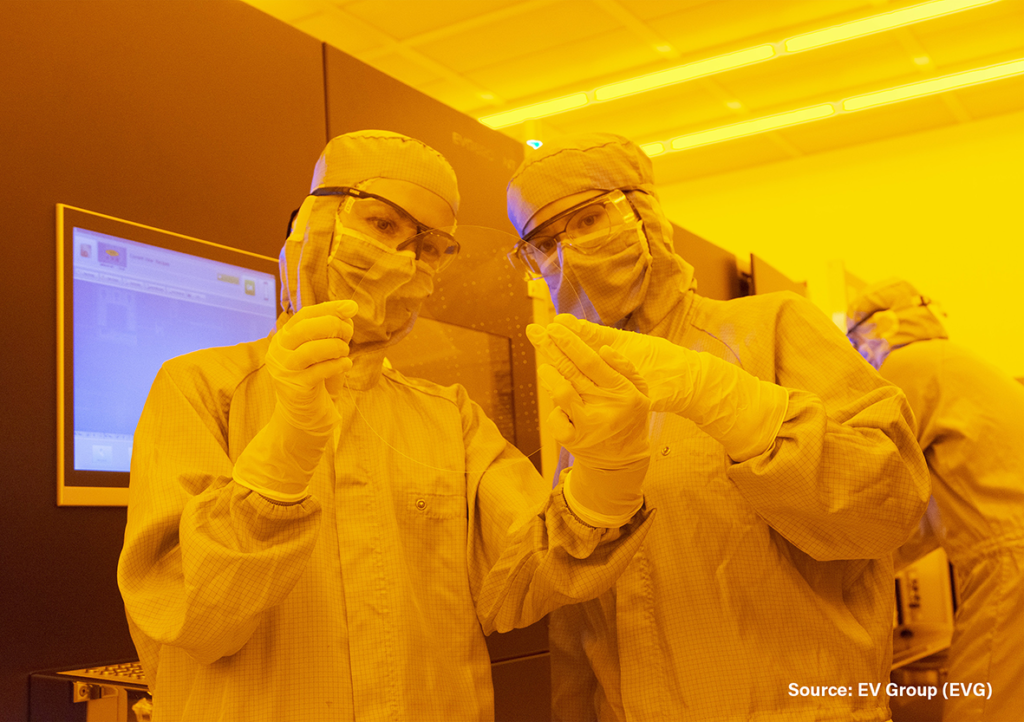
ASIA ELECTRONICS INDUSTRYYOUR WINDOW TO SMART MANUFACTURING
EV Group, Toppan Photomask Offer Nanoimprint Lithography for Photonics Manufacturing
EV Group and Toppan Photomask Co. Ltd. have entered into an agreement to jointly market nanoimprint lithography (NIL) as an enabling high-volume manufacturing (HVM) process for the photonics industry.
The collaboration combines the strengths of the leading supplier and pioneer of NIL systems and the leading supplier of photomasks to the semiconductor market. Specifically, it aims to establish NIL as an industry standard production process for photonics manufacturing. The partnership will accelerate NIL’s implementation in HVM to support a wide variety of applications. These applications include augmented/mixed/virtual reality headsets, smartphone and automotive sensors, as well as medical imaging systems.

Market NIL Development Kits
As part of this non-exclusive collaboration, EVG and Toppan Photomask will pool their knowledge, expertise and services to provide NIL development kits. These kits utilize master templates from Toppan Photomask and equipment and process development services provided by EVG. This aims to further promote NIL technology and its possibilities for industrial-scale implementation. In addition, EVG will offer NIL technology and product demonstrations to interested companies at EVG’s NILPhotonics® Competence Center at its headquarters in Austria. Furthermore, each company will designate the other as a recommended supply chain partner to companies interested in leveraging NIL to support their production needs.
“Toppan Photomask is very excited to enter into a collaboration with EVG”, said Chan-Uk Jeon, chief technology officer of Toppan Photomask Co., Ltd. “EVG’s NIL tooling and processing capabilities are world class and will enable cost-effective growth in photonics and other new technologies that are now adapting to NIL technology. Toppan Photomask sees a bright future as NIL grows into another successful lithography solution, enabled by both companies’ established strengths.”
Bringing Nanoimprint Lithography to Mainstream Manufacturing
Traditional lithography technologies are reaching their limits when it comes to addressing future applications that require the creation of small and arbitrarily shaped patterns, such as metalenses. NIL is a proven, cost-effective process for generating nanometer-scale-resolution patterns on complex structures, and thus is a viable alternative for these applications. NIL can replicate these complex structures very efficiently, on large areas, with fewer design constraints and a very streamlined process flow, for both prototyping and HVM.
EVG has been a pioneer in NIL technology for more than 20 years. It has helped to foster a wider NIL ecosystem through partnerships across the NIL supply chain – from suppliers of optical materials (such as adhesives and resists), substrate materials and stamp production to optical component and device manufacturers. With this collaboration between two established industry leaders in lithography and photomask fabrication, respectively, EVG and Toppan Photomask intend to fuel the adoption of NIL as a mainstream HVM technology for the photonics industry.
According to Markus Wimplinger, corporate technology development and IP director at EV Group, “We are excited to be partnering with Toppan Photomask to bring nanoimprint lithography to mainstream manufacturing applications. As the leading supplier of semiconductor photomasks with a reputation for the highest-quality standards, Toppan Photomask has extensive experience working with standardized production methods involving the world’s most stringent manufacturing requirements. This first-of-its-kind collaboration between a nanoimprint process equipment and services provider and a nanoimprint master manufacturer is a huge win for the industry and will aid our customers in quickly scaling up NIL as a mass-production technology for advanced optical devices and components – helping them to bring new ‘virtual’ ideas into reality.”
- Share: