ASIA ELECTRONICS INDUSTRYYOUR WINDOW TO SMART MANUFACTURING
Hitachi Eyes Patterned Wafers in New Inspection Tool
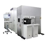
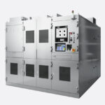
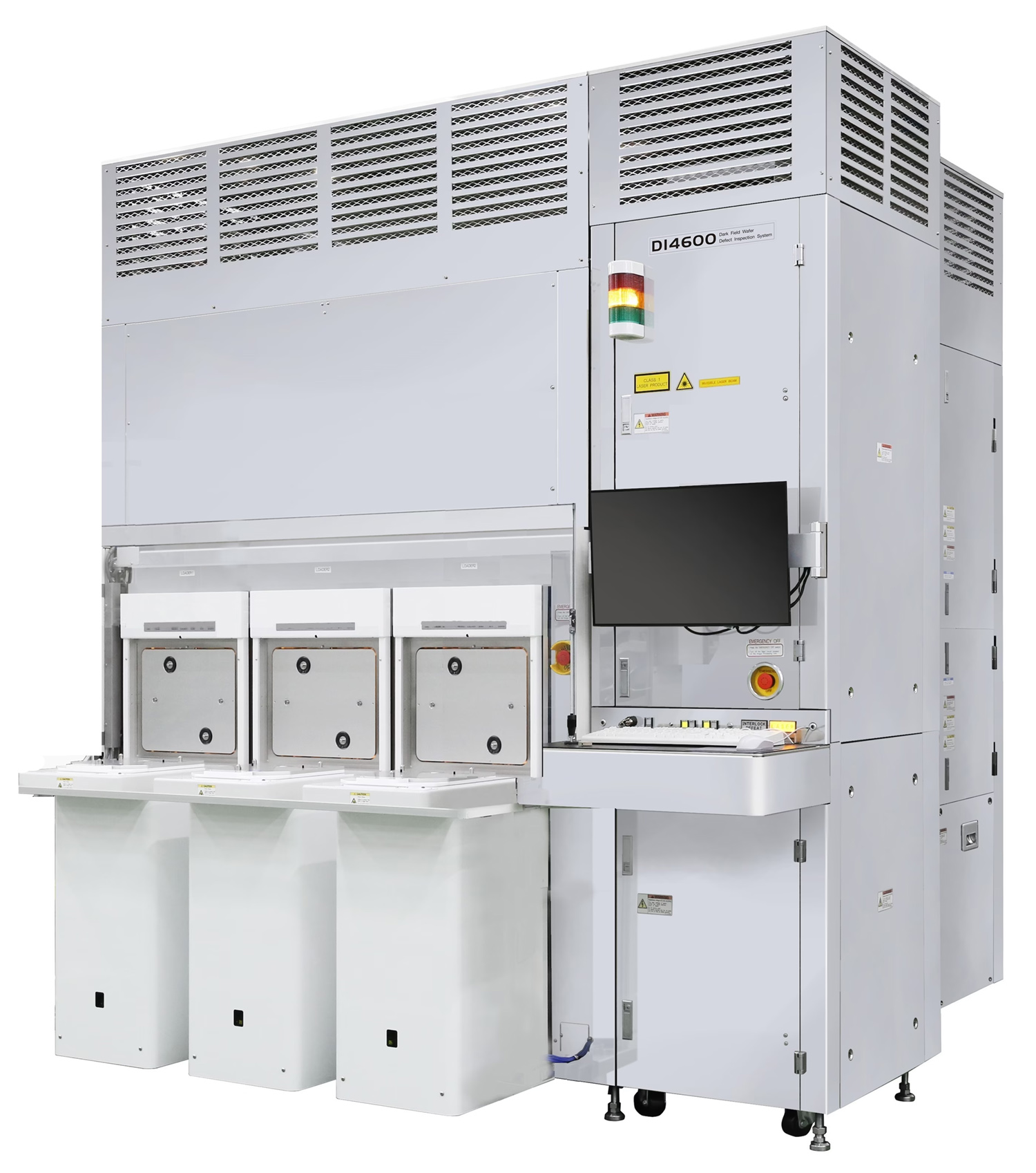
Hitachi High-Tech Corporation launches the Hitachi Dark Field Wafer Defect Inspection System DI4600. Specifically, this new tool suits the inspection of particles and defects on patterned wafers in semiconductor production lines.
Additionally, DI4600 offers improved detection capabilities due to the addition of a dedicated server. This server offers significantly enhanced data processing power required for the detection of particles and defects. Reduced wafer transfer time and improved operations during wafer inspection improve the system’s throughput by 20% compared to the previous model.
DI4600 will enable highly accurate defect monitoring in semiconductor production lines. Accordingly, it will contribute to improved yields and better cost of ownership as the semiconductor production volumes continue to expand going forward.
Development Background
In the current social environment, memory semiconductor devices, such as DRAM and FLASH, logic semiconductors, such as MPU and GPU are being used not only in smartphones, laptops, and PCs, but also for generative artificial intelligence (AI) computing and autonomous driving. As semiconductor devices shrinkage and complexity progresses, the requirements for manufacturing processes cleanness and inspection capabilities also become more rigorous.
Semiconductor manufacturers are constantly striving to improve their competitiveness, particularly when it comes to performance and manufacturing costs. Patterned wafer inspection tools contribute to yield management by inspecting the surfaces of production wafers for particles and defects. They allow engineers to monitor changes and trends of cleanness of semiconductor processing tools. Therefore, they have a great impact on semiconductor devices’ performance and manufacturing costs.
Key Technologies
1. High Throughput
Throughput has been improved by approximately 20% compared to the existing model. It reduces wafer transfer time, improves operations during wafer inspection and optimizes data-processing sequence.
2. High-Precision Detection
Detection precision has been improved due to the addition of a dedicated server that offers significantly enhanced data processing capabilities required for the detection of particles and defects.
By offering DI4600, as well as the company’s un-patterned wafer optical inspection systems and electron beam-based products such as a CD-SEM*1 and DR-SEM*2, Hitachi High-Tech is working to meet customers’ various needs in processing, measurement, and inspection throughout the semiconductor manufacturing process.
Hitachi High-Tech will continue to provide innovative and enhanced solutions to its products for the upcoming technology challenges. It will create new value together with its customers, as well as contribute to cutting-edge manufacturing.
*1 CD-SEM (Critical Dimension-Scanning Electron Microscope): An equipment designed to perform high-precision measurement of the dimensions of fine semiconductor circuit patterns formed on wafers.
*2 DR-SEM (Defect Review-Scanning Electron Microscope): An equipment designed to perform high-quality imaging of the defects on fine semiconductor circuit patterns formed on wafers.
- Share: