ASIA ELECTRONICS INDUSTRYYOUR WINDOW TO SMART MANUFACTURING
New TANAKA Gold Bonding Material Suits High-Density Chip Mounting
TANAKA Kikinzoku Kogyo K.K has established a gold particle bonding technology for high-density mounting of semiconductors using AuRoFUSE™ low-temperature fired paste for gold-to-gold bonding. Mainly, the company develops industrial precious metals products as one of the core companies of TANAKA Precious Metals.
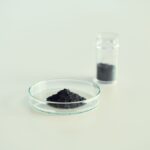
Specifically, AuRoFUSE™ is a composition of submicron-sized gold particles. It is a solvent that creates a bonding material with low electrical resistance and high thermal conductivity. Accordingly, it achieves metal bonding at low temperatures.
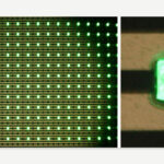
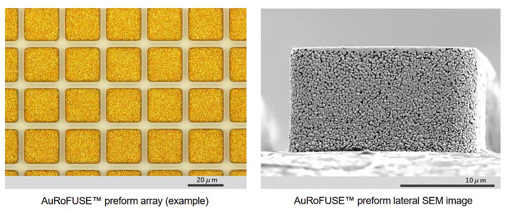
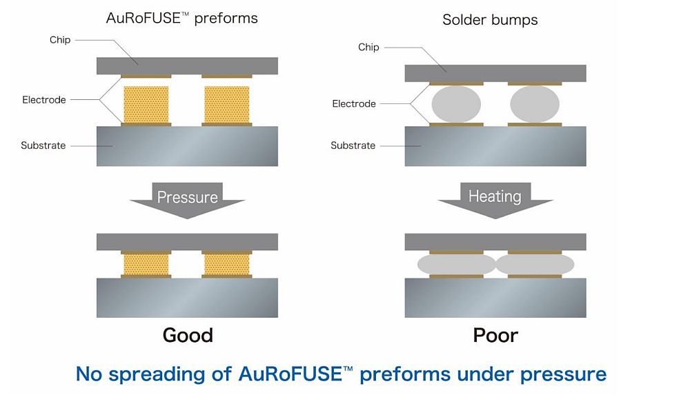
Using AuRoFUSE™ preforms (dried paste forms), this technology can reach 4μm fine-pitch mounting with 20μm bumps. They are formed through a thermocompression bonding process (20MPa at 200°C for 10 seconds). Thus, AuRoFUSE™ preforms exhibit compression of approximately 10% in the compressive direction while showing minimal deformation in the horizontal direction. This gives them sufficient bonding strength1 for practical applications, making them suitable for use as gold bumps2. With the main component being gold, which has a high level of chemical stability, AuRoFUSE™ preforms also provide excellent reliability after mounting.
Additionally, this technology enables miniaturization of semiconductor wiring and greater integration (higher density) for various types of chips. It is expected to contribute to the high-level technical innovation required of advanced technologies. Among them are optical devices such as light-emitting diodes and semiconductor lasers, as well as personal computers, smartphones, and in-vehicle components.
TANAKA will actively distribute samples of this technology in the future to promote greater awareness in the marketplace.
TANAKA will present this technology at the 38th Spring Conference of the Japan Institute of Electronics Packaging to be held from March 13 to 15, 2024, at the Tokyo University of Science.
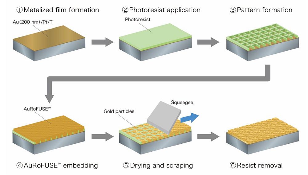
Manufacturing of AuRoFUSE™ preforms
(1) Au/Pt/Ti metallization of the bonding substrate to form the base layer
(2) Photoresist applied to the bonding substrate after metallization
(3) Exposure/development by holding the photomask, corresponding to the preform shape, over the bonding substrate to form a resist frame
(4) Flowing of AuRoFUSE™ into the formed resist frame
(5) Vacuum drying at room temperature, followed by scraping off excess gold particles with a squeegee3
(6) Temporary sintering through heating, followed by separation and removal of the resist frame
Achieving High-Density Mounting with AuRoFUSE™ Preforms
Depending on the purpose, various bonding methods are used for mounting semiconductor devices, including solder and plating methods. The solder-based bonding method is a low-cost, speedy method of producing bumps. However, because solder tends to spread outward when melted, there are concerns about possible short-circuiting through contact between electrodes as the bump pitch becomes finer. In the development of technologies for high-density mounting, electroless plating4 is becoming mainstream for producing copper and gold plating bumps. This method can achieve a fine pitch, but because comparatively higher pressures are required during bonding, chip damage is possible.
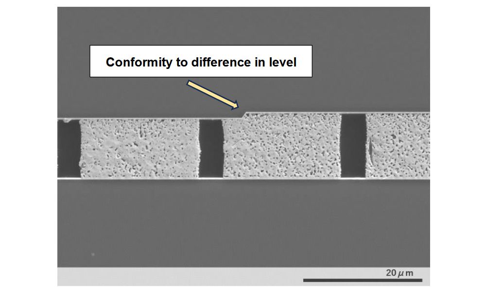
As precious metals professionals, TANAKA Kikinzoku Kogyo has been conducting research and development into the use of AuRoFUSE™. Specifically, it enables low-temperature, low-pressure bonding with followability of uneven surfaces due to its porousness. As a result, it achieves high-density mounting of semiconductors. Mainly, the company initially attempted to use the mainstream application methods of dispensing5, pin transfer6, and screen printing7. However, the fluidity of the paste made those methods unsuitable for high-density mounting.
Using this new technology, the paste is dried prior to bonding to eliminate fluidity, which minimizes spread and enables high-density mounting (Figure 1). Also, the porous structure of the paste makes it easily formable as well. This enables bonding even when there is a difference in height between electrodes or differences in warpage or thickness of the substrate (Figure 2).
References:
AuRoFUSE™ is a paste-type bonding material containing a mixture of gold particles, with the particle diameter controlled to be submicron sized, and an organic solvent. Generally, microscopic particles have a characteristic called “sintering” where particles bond to each other when heated to a temperature under the melting point. If AuRoFUSE™ is heated to 200°C, the solvent evaporates, and the gold particles undergo sinter bonding without the application of a load, providing sufficient bonding strength of approximately 30MPa.
Notes:
[1] Bonding: Refers to shear strength (strength determined through application of a lateral load during testing)
[2] Bumps: Protruding electrodes
[3] Squeegees: Tools made from rubber or polyurethane resin that are used to scrape off excess material
[4] Electroless plating: Refers to plating applied through a chemical reaction without using electricity; it enables plating of certain metals and precious metals, including copper, gold, nickel, and palladium
[5] Dispensing: A paste application method that uses a dispenser to spray a fixed amount of a liquid
[6] Pin transfer: A paste application method like stamping with multiple pins
[7] Screen printing: A paste transfer method whereby a screen mask is formed in any printed pattern, paste is applied, and scraped off with a squeegee to reveal the pattern
- Share: