ASIA ELECTRONICS INDUSTRYYOUR WINDOW TO SMART MANUFACTURING
Novel Crystal β-Ga2O3 Offers Better Alternative to SiC, GaN
Novel Crystal Technology, Inc. (NCT), a carve-out venture of Tamura Corp. and a technology transfer venture from Japan’s National Institute of Information and Communications Technology (NICT), reports it is conducting research and development of β-type gallium oxide (β-Ga2O3). Specifically, β-Ga2O3 is a promising candidate for semiconductor material in new-generation power devices. Mainly, gallium oxide power devices with medium to high breakdown voltage are highly expected to contribute to energy saving.
Characteristics of β-Ga2O3
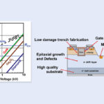
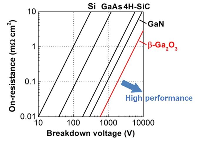
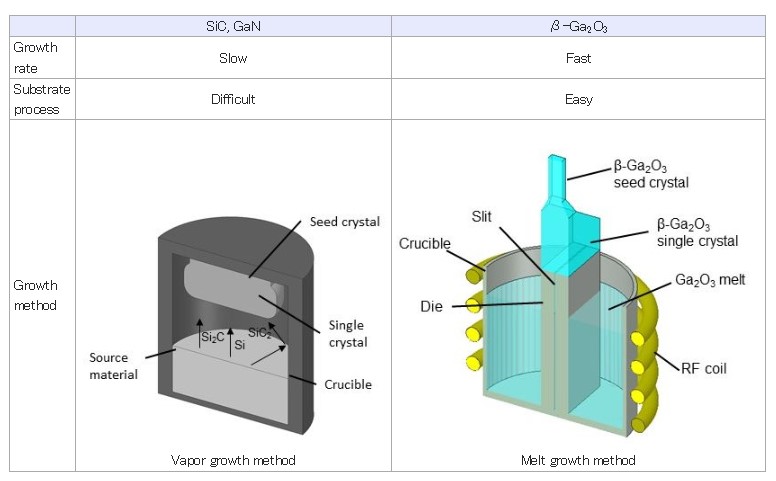
Primarily, β-Ga2O3 is a new semiconductor material for power devices and has larger band-gap energy than silicon carbide (SiC) and gallium nitride (GaN). Therefore, it can be used to create semiconductor devices that can withstand high voltages and low resistance. In addition, since growing β-Ga2O3 single crystal forms a melt, providing high-quality substrates with low cost than SiC and GaN is possible.
Paves Way for Larger Wafer for Ga2O3-based Power Devices
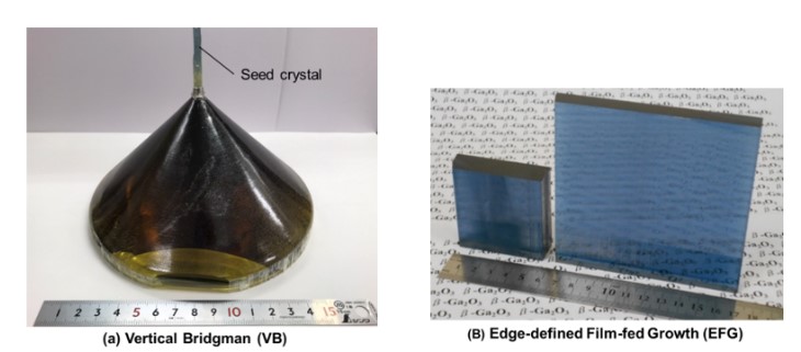
Recently, Novel Crystal also announced it has successfully grown the first 6-inch Ga2O3 single crystal using the advanced Vertical Bridgman (VB) technique. This achievement marks a significant step forward in NCT’s efforts to deliver larger, high-quality semiconductor wafers for Ga2O3-based power devices.
Primarily, the VB technique offers several advantages over Novel Crystal’s existing Edge-defined Film-fed Growth (EFG) method. By growing the crystal in a cylindrical shape, VB significantly reduces costs associated with substrate cutting. Additionally, it allows for production of substrates in various crystalline orientations, unrestricted by limitations imposed by crystal anisotropy. Furthermore, the controlled thermal environment of VB growth leads to superior crystal quality with minimal defects, compared to EFG. Finally, dopant uniformity within the substrate is expected to improve, aligning with industry standards for other semiconductors like silicon.
Quest for Larger Substrates
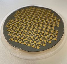
Established in 2015, NCT manufactures 2-inch and 100mm gallium oxide (Ga2O3) substrates and epi-wafers for power devices. These are commercially available and used by universities, institutes, and power device companies worldwide. Currently, NCT supplies thousands of these substrates annually to support research and development efforts.
Moreover, NCT is actively developing larger substrates such as 6-inch. Beyond substrates, NCT has a vision for broader Ga2O3 device production. They are already offering samples of their first Ga2O3 Schottky Barrier Diode (SBD), with qualification tests expected to be completed in September 2024.
The development of the Vertical Bridgman growth technique for Ga2O3 single crystals was initiated by Shinshu University. Specifically, it successfully achieved growth of 2-inch and 4-inch crystals. NCT acquired and extended their techniques to enable larger diameter crystal development. Particularly, this research and development program was partially funded by the Adaptable and Seamless Technology Transfer Program through Target Driven R&D (A-STEP) of the Japan Science and Technology Agency (JST).
-26 April 2024-
- Share: