ASIA ELECTRONICS INDUSTRYYOUR WINDOW TO SMART MANUFACTURING
Ams Osram Eyes to Have New Fab in Austria
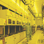
ams OSRAM is sustainably strengthening its development and production site in Premstätten in Austria. Specifically, the company is bracing for a EUR588 million in investments spread until 2030, which will include the construction of a new fab facility in Styria.
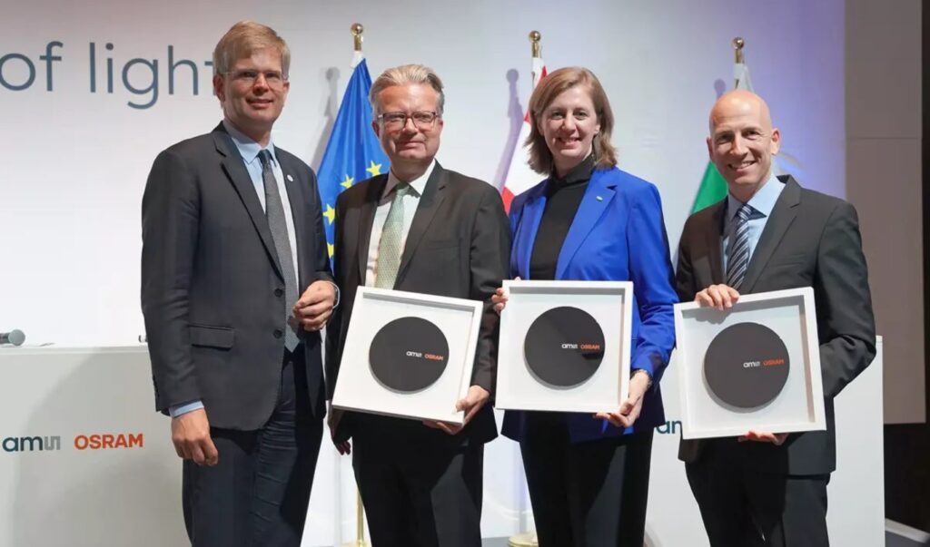
Aldo Kamper, CEO of ams-OSRAM AG, along with Federal Minister Martin Kocher and Styria Governor Christoper Drexler announced the investment plan. The company has already applied for funding of up to EUR200 million as part of the European Chips Act program.
The planned new factory at the production site in Styria will further expand the leading role of the Austrian semiconductor industry. Moreover, this will create a total of 250 new jobs in the next few years.
More Innovation, More Made-in-Europe Products
The global situation in the semiconductor market clearly shows the importance of investing in innovative key technologies for the future. For that reason, the European Commission has set itself the goal of promoting the mass production of semiconductors in Europe. Furthermore, increasing its global market share to 20 percent of production by 2030.
In addition, next-generation chip technologies will emerge. This prompted the region to introduce the European Chips Act.
The investment by ams OSRAM will help strengthen European sovereignty in semiconductor production and digitization. It will also make an important contribution to the “Green Transition”.
“With the new factory at our headquarters, we can create more space for innovation, meet the growing needs of our customers and manufacture more products in Europe,” says Kamper.
“At the same time, our investment is a clear commitment to Premstätten as a business location, to Styria as a high-tech location, and to Austria as a location for innovation and production. From here, we are driving forward digitalization in line with the European Green Deal and supporting Europe’s technological sovereignty.”
First of Its Kind
Meanwhile, as part of its strategic program ‘Re-establish the Base’, ams OSRAM is focusing on structural growth areas. Specifically, it is focusing on intelligent sensors and emitters. Moreover, with highly differentiated components for consumer handhelds.
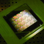
The planned semiconductor manufacturing facility, which will be the first of its kind in the world. Accordingly, it will produce the next generation of highly differentiated optoelectronic sensors for medical and automotive applications. There are also plans to manufacture products for industrial and consumer goods applications.
Furthermore, it consists of a combination of outstanding technologies (CMOS, Filter¹⁾ and TSV²⁾) functions according to a toolbox concept.
Notes
¹⁾ Filters select incoming radiation. For example, they use the phenomenon of interference – the overlapping of light wavelengths. That is, to pass or reflect certain spectral ranges of electromagnetic radiation. This enables color recognition beyond that of the human eye,
²⁾ TSVs – Through Silicon Vias – are vertical electrical connections through a chip. They are essential building blocks for advanced packaging technologies for high performance, small footprint devices required in many different market segments.
16 May 2024
- Share: