ASIA ELECTRONICS INDUSTRYYOUR WINDOW TO SMART MANUFACTURING
Multibeam Debuts First Multicolumn E-Beam Lithography
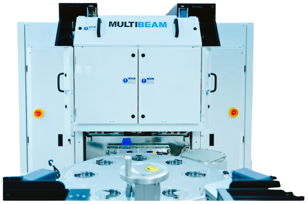
Multibeam Corp. has introduced the MB platform, a first-of-a-kind Multicolumn E-Beam Lithography (MEBL) system built for mass production. This development is a milestone for the global semiconductor industry.
Particularly, the fully automated precision-patterning system suits rapid prototyping, advanced packaging, high-mix production, chip ID, compound semiconductors, and other applications. SkyWater Technology will use the system for early concept prototyping and rapid production of microchips.
Revolutionizes E-Beam Lithography
Multibeam’s platform revolutionizes e-beam lithography (EBL) with new productivity advantages. The company achieved this while enabling high resolution, fine features, wide field of view, and large depth of focus.
Mainly, the chief productivity driver is the novel architecture that employs multiple miniature columns, which operate individually and in parallel. Also, it features an advanced control system directing the beams to achieve maximum accuracy, quality, and speed.
Additionally, throughput is more than 100 times greater than conventional EBL systems. This makes the MB platform the highest productivity high-resolution maskless lithography system on the market.
Primarily, it gives manufacturing leaders a breakthrough solution to enable rapid development of new IC designs, faster time to market, and accelerated IC innovation.
The platform was developed by a team of semiconductor equipment and patterning technology experts led by industry pioneer, Dr. David K. Lam. Mainly, it is the first EBL system designed from the ground up for volume production-the first one innovated in Silicon Valley and the first built by a U.S. lithography company to emerge in decades. With the launch, Multibeam becomes the sole domestic supplier of EBL technology.
“We are thrilled to introduce the MB platform and proud to send our first production system to SkyWater,” said Multibeam’s Chairman and CEO, Dr. David K. Lam.
“The semiconductor industry’s growth continues to be fueled by exciting new applications, with advanced lithography technologies enabling endless innovations. At the same time, there is soaring growth in markets like AI and edge computing, where the enablers include purpose-built silicon and advanced packaging. Also, the manufacturers’ priorities are rapid cycles of learning and cost-effective, seamless transition to production for faster time to market. For these emerging markets, the MB platform offers a complementary lithography solution. With powerful productivity advantages, it unleashes EBL’s full precision-patterning capacity and expands the range of lithography options available to IC leaders.”
From Development to Manufacture of MEBL
Primarily, the launch marks Multibeam’s shift from development stage to producer of high-productivity Multicolumn E-Beam Lithography systems. While EBL is valued for its patterning capabilities, low throughput constrains its capacity to take emerging applications from R&D to production. To unlock the potential, Multibeam re-innovated EBL leveraging well-established technologies to reduce risk.
As the MB platform evolved, new applications were emerging with technical, economic, and time-to-market imperatives that could be effectively addressed by a maskless lithography solution.
“This dynamic affirmed our conviction that an EBL system, re-engineered for high productivity, could enable applications at advanced nodes for the first time,” said Multibeam President, Dr. Ken MacWilliams.
“The performance advantages are especially compelling in advanced packaging where our system can enable improvements in chip-to-chip power, along with bandwidth and latency. This is helping to drive a new technology inflection that the industry is starting to call ‘advanced integration’ — where new chip-to-chip interconnects can achieve comparable performance to on-chip interconnects.”
“We are proud to enable this inflection with a production-proven lithography solution, and confident that our system will help chipmakers seize profitable new market opportunities,” said MacWilliams.
EBL: Re-Innovated for Ultra-High Productivity
Mainly, the team designed the platform from the outset for volume production, and more than 40 patents protect the innovations. In addition to the multicolumn vector-writing architecture, which drives productivity, accuracy, and speed, the platform offers auto wafer loading and alignment from wafer cassette to the exposure process in the system.
Also, an automated vacuum recovery system optimizes uptime, along with a speedy column replacement process and calibration technology. The advanced automation capabilities reduce operator requirements and further contribute to the system’s cost-of-ownership benefits.
As a maskless lithography solution, the platform offers additional advantages. Where it can take weeks to develop optical masks, designs can be written in hours with the MB platform. This gives manufacturers greater IC design latitude, while reducing costs and accelerating time to market.
To further enable design flexibility, the platform leverages technology from EDA leader, Synopsys, to generate write recipes, which lets customers achieve their most intricate patterns. With a powerful built-in data prep system, developed in conjunction with Synopsys, the system writes the chip layouts directly onto wafers without masks.
Finally, with a compact footprint, the system has lower power requirements and needs less fab space. Also, modular by design, it easily adds modules as needed for new applications or even higher throughput. In addition, it is fully self-contained and requires no special environment, which further reduces costs. The system is available in 150mm, 200mm and 300mm configurations.
-01 July 2024-
