ASIA ELECTRONICS INDUSTRYYOUR WINDOW TO SMART MANUFACTURING
Toyo Technica Pitches New AI-Equipped FIB-SEM
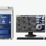
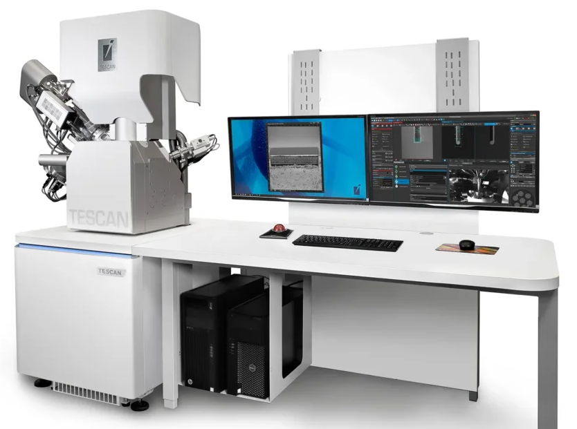
Toyo Technica Co., Ltd., a Japanese trading company specializing in measuring equipment, has released of the new Xe plasma FIB-SEM “AMBER X 2” manufactured by TESCAN GROUP, a.s. (Headquarters: Brno, Czech Republic).
Mainly, the new AMBER X 2 highlights the integration of AI technology. As a result, it fully automates the preparation of transmission electron microscopy (TEM) samples (*1), which requires skilled technology. Also, it further improves the throughput of large-area processing, which is a feature of plasma FIB. Accordingly, this will contribute to the development of a wide range of materials, including electronic devices, lithium-ion batteries, soft materials, and magnetic materials.
This product was introduced first in Japan at JASIS 2024 starting September 4.
Overview/Background
FIB-SEM (Focused Ion Beam Scanning Electron Microscope) is an analysis system that integrates a focused ion beam system (FIB) that can perform cross-sectional processing of microscopic areas and an electron microscope (SEM) that enables high-resolution observation. It confirms the internal structure and cross-sectional structure of samples during the development of high-performance materials and electronic devices or when investigating the cause of defects.
In recent years, there has been a wide range of materials that need to be analyzed. Further, the areas to be analyzed have expanded. Thus, in addition to high-precision processing and observation technologies, further efficiency of work is required.
Toyo Technica’s AMBER X 2 also features a column with improved FIB high-current performance(*2). Specifically, this enables high-speed processing of targeted areas with nanometer-order positional accuracy, even in large areas. In addition, it integrates a fully automated software using AI technology for the preparation of TEM samples to be analyzed. Accordingly, this enables the production of high-quality TEM samples without the injection and contamination of Ga ions seen in FIBs using conventional gallium (Ga) ion beams.
In the past, there were many steps involved in TEM sample preparation, and it took time to learn the skills. However, this fully automated software using AI technology makes it easy to prepare samples without relying on skills. With this system, it is possible to further improve processing performance and improve the efficiency of sample preparation.
*1 TEM sample: Sample used in the Transmission Electron Microscope
*2 FIB column: A mechanism that focuses and scans ion beams drawn from an ion source into thin strips and irradiates the sample.
Main Features of Xe Plasma FIB-SEM “AMBER X 2”
・Composite system that integrates FIB and SEM using Xe (xenon) plasma as an ion source;
・High beam current (up to 3.3μA) of plasma Xe ions enables large-area (up to 1mm width) FIB cross-sectional processing Fast
・Nanometer-order positional accuracy makes it easy to finely process the target area
・Ga-free sample preparation enables analysis without damaging the sample.
This is an online translation of a Japanese press release with slight editing by Dempa.
-05 September 2024-
- Share: