ASIA ELECTRONICS INDUSTRYYOUR WINDOW TO SMART MANUFACTURING
IC Packaging Group Boosts Might, Adds 3M as New Member
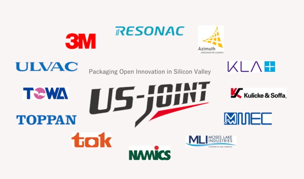
Resonac Corporation has welcomed the addition of 3M Company (ST. PAUL, Minn. United States) as a new member of the US-Joint consortium. Accordingly, with this addition, US-JOINT now comprises 12 companies from Japan and the United States.
Resonac took the lead in the establishment of the US-JOINT consortium*1 for next-generation semiconductor packaging.
“As the demands of AI and other high performance computing technologies increase, suppliers must work together to provide comprehensive solutions to tough challenges on increasingly shorter timelines.” said Steven Vander Louw, 3M’s president of display and electronics product platforms.
Represents Japan, U.S. Innovations
In addition, Louw said the companies in the US-Joint Consortium represent U.S. and Japanese innovation leaders in a range of advanced packaging technologies. “3M is pleased to join the consortium in order to bring our decades of materials science expertise, across more than 50 technology platforms, to help address these challenges,” said Louw.
With 3M, this means the group will be adopting 3M’s decades of materials science expertise, across more than 50 technologies and platforms. Thus, propelling further US-JOINT consortium’s research and development on next-generation semiconductor packaging.
“We are delighted to welcome 3M to the US-JOINT Consortium,” said Hidenori Abe, Corporate Officer, CTO for semiconductor materials, Resonac. “3M’s expertise in materials science and commitment to innovation in advanced packaging device and process solutions will be an asset as we work together to solve difficult technical and integration challenges for customers onshore in the United States.”
Next-generation semiconductors, particularly those aimed at the rapidly growing AI market, are achieving enhanced performance through cutting-edge packaging technologies such as 2.5D and 3D*2. In recent years, not only semiconductor manufacturers but also major tech companies, including GAFAMhyperscalers and fabless companies, have been creating the latest concepts in semiconductor packaging. US-JOINT will collaborate with these companies to validate the latest concepts in semiconductor packaging. US-JOINT plans to establish a research and development center equipped with clean rooms and manufacturing equipment in Silicon Valley, and commence operating it by the end of 2025.
Moving forward, Resonac will continue conducting research and development on cutting-edge packaging technologies that support the evolution of semiconductors in collaboration with US-JOINT.
Notes:
*1. News release regarding the establishment of US-JOINT
https://www.resonac.com/news/2024/07/08/3116.html
*2. 2.5D packaging is a technology to place semiconductor chips in parallel on the silicon substrate, which is called “interposer.” 3D packaging is a technology to stack chips.
- Share: