ASIA ELECTRONICS INDUSTRYYOUR WINDOW TO SMART MANUFACTURING
ASE’s New Chip Package Tech Suits AI, HPC Demands
Artificial intelligence and high performance computing (HPC) are making headway across many industries. In fact, the convergence of AI and HPC has brought huge impact as well on the manufacture of semiconductors.
Semiconductors are critical to the enablement of AI and HPC, which are crucial to applications from autonomous vehicles and even in medical field. For that reason, semiconductor manufacturers need to roll out innovative semiconductor packaging solutions to meet the growing demand high-bandwidth data transfers.
Advanced Semiconductor Engineering, Inc. (ASE) has announced its new Fan-Out Chip-on-Substrate-Bridge (FOCoS-Bridge) with Through Silicon Via (TSV). Accordingly, the new packaging technology will enable further AI and its emerging impact across industries.
ASE’s FOCoS-Bridge with TSV addresses growing demand for increased bandwidth by creating a shorter delivery path through TSV and enabling a higher I/O density and enhanced thermal dissipation. Thus, delivering critical performance improvements.
The integration of TSV expands ASE’s VIPack™ FOCoS-Bridge capabilities to deliver critical energy efficiency at a time when the need has never been greater across emerging AI and high-performance computing (HPC) applications.
How FOCoS-Bridge Innovate Semiconductors?
FOCoS-Bridge technology can help to meet the increasing demand for higher bandwidth and faster data transfer rates in AI and HPC applications. Therefore, this technology is emerging as a promising semiconductor packaging solution.
Specifically, it leverages the advantages of highly integrated fan-out structures to overcome the limitations of traditional electrical interconnects, and enables high-speed, low-latency, and energy-efficient data communication between processors, accelerators, and memory modules.
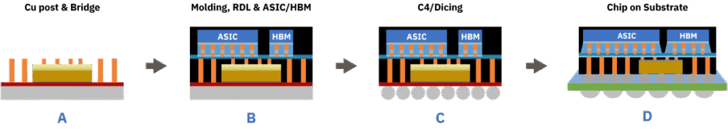
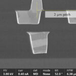
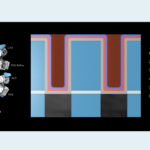
The technology utilizes tiny silicon pieces with routing layers as in-package interconnect between chiplets, such as graphics computing chips (GPU) and high bandwidth memory (HBM). The silicon bridges are embedded in the fan-out redistribution layers (RDLs).
The TSV bridge chips provide a new shorter vertical path for power delivery in conjunction with traditional lateral signal connections. The TSV and passive devices are embedded and interconnected using three RDLs with 5µm line and space. When compared to FOCoS-Bridge, the resistance and inductance of FOCoS-Bridge TSV are significantly reduced by 72% and 50%, respectively.
Therefore, the VIPack FOCoS-Bridge platform can help improve power integrity and provide direct access for improved performance.
FOCoS-Bridge is positioned as an alternative to 2.5D packages using silicon interposers. Like 2.5D, silicon bridges provide ultra-fine pitch interconnection in packages, which can address the memory bandwidth bottleneck challenges in systems. Unlike 2.5D technology, FOCoS-Bridge offers the advantage of using silicon pieces only in the specific areas where two chiplets are being connected.
Advances Packaging to Next Level
Yin Chang, Executive Vice President at ASE. “Our introduction of the FOCoS-Bridge with TSV underscores ASE’s strategic commitment to supporting the AI ecosystem with advanced heterogeneous integration solutions. This innovation enhances our VIPack portfolio, offering a scalable, high-density packaging platform optimized for sustainable, high-performance computing architectures.”
On the other hand, Teck Lee, Director of R&D at ASE said by incorporating TSV, FOCoS-Bridge enhances compute and energy efficiency, and elevates our advanced packaging portfolio to the next level. He added ASE’s FOCoS-Bridge capabilities enable seamless integration of SoCs and chiplets with high-bandwidth memory. Thus, meeting the need for greater computational performance of HPC and AI applications.
FOCoS-Bridge technology has already demonstrated its ability to address higher bandwidth and faster data transfer rates in AI and HPC applications. It leverages the advantages of highly integrated fan-out structures to overcome the limitations of traditional electrical interconnects, and enables high-speed, low-latency, and energy-efficient data communication between processors, accelerators, and memory modules.
While establishing the foundation for embedding passives and active chips in the fan-out package, FOCoS-Bridge also provides options of decoupling capacitor integration for power delivery optimization and active dies for interconnection between to certain functions, such as memory, I/O, and more.
30 May 2025
- Share: