ASIA ELECTRONICS INDUSTRYYOUR WINDOW TO SMART MANUFACTURING
Data-Guzzling Applications Drive Innovations Across Chip-Making Processes
Global chip industry is facing the toughest technological challenges ever, as the industry is now undergoing the most disruptive changes in chip structure, raw materials, chip-making technology and equipment, and even chip packaging technologies.
For one thing, chip makers are now rapidly adopting a new generation of EUV photolithography equipment, as they are necessarily required to shrink down the width of a chip below 10 nanometers to put more of transistors into a given space of silicon wafer.
The ramp-up to EUV, extreme ultra violet technology is in turn calling for dramatic changes in every layer of the ecosystem from raw materials for pellicles to photo masks to photo resist to even light source equipment.
Chip structure is also changing from planar one into 3D FinFET shape to reduce heats dissipation, as a progressively smaller and smaller transistor gate is so vulnerable to current leakages that it can disrupt chip performances and power consumption.
As data transferring or sharing is increasingly important between chip components like memory chips and CPUs, heterogeneous integration is emerging as a new technology challenge, calling for disruptive innovations in the chip packaging technology including 3D TVS as well as Fan-in and Fan-out chip packaging technologies.
All combined, underlying these disruptive changes in the chip structure, equipment, raw materials, chip fabrication and even packaging technologies are the proliferation of real-time and data-guzzling applications like AI, IoT, 5G and autonomous driving.
Ramp-up to EUV
All of these applications are clamoring for tones of data moving back and forth between devises in real time to see, feel, hear, analyze, predict, and finally dictate what to do next, guzzling more of computing power and data storage spaces.
This helps explain why chip makers are struggling to embed more of transistors into a chip -The smaller a transistor, it can embed more of them, the faster it can process data, consuming less power.
According to a paper published by the Journal of Micro-Nanopatterning Materials and Metrology, EUV lithography will prevail as a de facto chip scaling technology at least until 0.75nm by 2034.
EUV is a sort of light source, of which wavelength is as short as 13.5nm -short enough to allow chip makers to draw as thin fine pitches as 7nm and below on a silicon wafer. As chip makers can draw such thin patterns on a wafer, it allows them to put 25% more of transistors at a given space of silicon wafer than predecessor ArF-based double patterning lithography technology.
Samsung and TSMC pioneered the industry’s ramp-up to EUV equipment in 2018, using ASML’s 0.33 NA (numerical aperture) EUV scanner to fabricate 7nm circuitry-wide logic chips.
Both of the two chip makers are now fabricating logic chips of 5nm-wide circuitry using ASML’s EUV equipment, and the two rivals are competing head-on to reach a 3nm chip circuitry technology ahead of the other.
Memory chip makers like Samsung and SK hynix have been even implementing EUVs to fabricate DRAM chips of 10nm-level circuitry, as the industry is rapidly ramping up to speedier DDR5 to meet strong demand for far wider memory bandwidth across data-hungry applications like AI and IoT.
Looking forward, analysts predict that current 0.33 NA EUV equipment will outlive until 2025 when the industry can attain 1.5nm chip circuitry technology using double patterning methodology.
Over the next 10 years since then, the industry is expected to begin its struggle to implement a next generation of high NA EUV, which uses 0.55 NA lens, to ramp up to 0.75nm circuitry technology by 2034.
Other lithography technology in developments include DSA, direct-write lithography and nanoimprint.
From 2D Planar to 3D
Yet, the photolithography technology isn’t the only option to shrink down chip circuitry to an atom level.
More innovations in chip structure, materials, and tools are strongly need, too, as the continuous ramp up to finer circuitry technology necessarily creates side-effects.
The race between Samsung and TSMC for a 3nm circuitry technology helps explain why chip makers are struggling to change 2D planar chip structure into 3D shape.
The 3D FinFET chip structure was commercialized in the first half of 2010s to tackle what’s called as “short channel” effects, the excessive heats dissipation phenomenon.
True enough, chipmakers have been struggling to solve the leakage current phenomenon for years, as electrons more tend to derail out of their course between source and drain regions as the in-between gate width gets narrower and narrower.
Wrapping the gate around multiple channels, the 3D FinFET structure can solve the problem at 14nm, 10nm and 7nm wide nodes
As the node gets as narrow as 5nm and 3nm, the conventional 3D FinFET structure faced difficulties in controlling leakage current and other short channel effects. It calls for evolutions of the FinFET technology.
Leading the evolution is Samsung Electronics that has commercialized MBCFET, or multi-bridge channel filed effect transistor-structured logic processor chips of 3nm nodes.
The MBCFET is an advanced version of GAA FET or gate all around FET structure, under which a gate material surrounds nanowire channel regions from all sides.
What make differences with GAA FET is that Samsung vertically stacks nanosheets, rather than nanowires to form channel regions and then surrounds them with a gate from all sides to create MBCFET structure. Designed to be used in applications from low power to high performance, the MBCFET requires cutting-edge innovations in material technology such as nanosheet and high-k metals, for example.
The innovation translates into 50% power savings, 30% performance improvements, and 45% area reduction, compared with the 7nm FinFET process.
Stacking Dies on 3D package
TSMC is also working with the GAA structure in its ramp-up to a 3nm circuitry technology. Intel is developing MBCFET nanoribbon transistor.
Chip packaging technology has been evolving from 2D planar to 3D structure, too, as chip makers have been struggling to embed multiple of discrete and different dies like CPUs, GPUs, and memory chips into a single package in what’s called as heterogeneous integration.
The idea is to replace prohibitively expensive SoC solution with relatively cheaper SiP or system in package solution to save costs and improve functionalities.
At issue is how to interconnect different devices efficiently with more of IOs and less heat dissipation to ensure lightweight smaller form factors, low data latency, lower power requirements per function and lower costs.
Leading the way is TSMC that implements various 3D packaging systems under a trademark of 3DFabric. TSMC has lined up wafer-level package technologies CoWoS, , InFO (integrated fan out), SoIC CoW (chip on wafer) and SoIC WoW (wafer on wafer).
InFo is an innovative wafer level package system that integrates application processors and mobile DRAMs on a package level using RDL or re-distribution layer and TIV or through InFo Via.
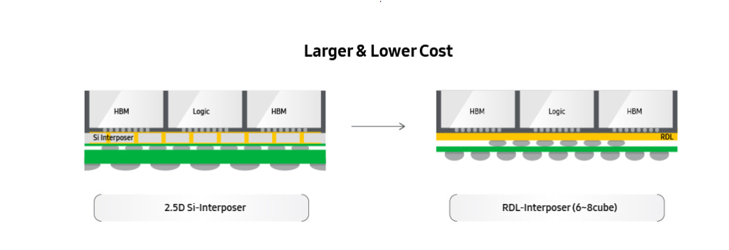
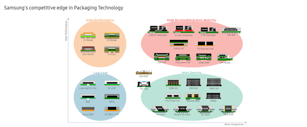
Samsung Electronics is also working on a variety of 2.5D and 3D packaging solutions for high performance applications, including 2.5D packaging technology Interposer-Cube 4 (I-Cube4), FO-SiP, i-PoP, and FOPLP-PoP.
For example I-Cube 4 is a sort of packaging technology to integrate one or more logic dies like CPUs and GPUs and high bandwidth or HBM memory dies on a paper-thin silicon interposer. It allows many different dies to work I one single package as if it is a single chip.
It comes built with a unique mold-free structure for the I-Cube 4 solution, which incorporates four HBMs with one logic die, for better thermal management and stable power supply.
- Share: