ASIA ELECTRONICS INDUSTRYYOUR WINDOW TO SMART MANUFACTURING
Samsung to Produce 3nm Logic Chips in 2022
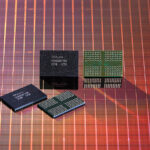
Samsung Electronics said on Oct. 6 that it will start mass-production of 3nm logic chips sometime in the first half of 2022, using a GAA, or gate all around 3D chip-fabrication technology.
The roadmap runs several months ahead of foundry chip market leader TSMC’s ramp-up schedule to start the commercial roll out of the same 3nm node logic chip in July 2022, declaring Samsung a winner in the years-long tug-of-war to outstretch each other in the chip node shrinking technology race.
As an annual Samsung Foundry Forum 2021 held online on Oct. 7, Samsung unveiled its ambitious technology ramp-up plan that calls for the world’s second largest foundry chip maker to scale all the way through 5nm to 3nm and 2nm chip node process technology.
According to the ramp-up plan, Samsung is scheduled to attain an early version of 3nm chip node technology in the first half of 2022 and then an advanced version of the 3n technology in 2023. By 2025, the roadmap indicates that Samsung will ramp up to a 2nm chip node technology, using a nanosheet-based GAA FET technology.
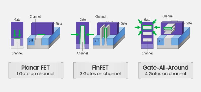
A short for gate all around filed effect transistor, the GAA FET technology is basically a nanosheet transistor with a gate getting all around it. As a gate is placed in all four sides of the channel, it have a strong control over channel, better short channel effect, high conductivity, and better electrical properties.
The technological advantage translates into a 30% chip performance, a 50% cut in power budget, a 30% shrinkage in the chip footprint, compared with a FinFET 5nm chip node technology.
GAA FET is a successor to 3D FinFET chip-making technology which is designed to tackle challenges in scaling down below 5nm node without compromising chip performances.
Meanwhile, Samsung also unveiled another technology innovation -17nm 3D FinFET chip process technology that is to be used mainly to fabricate CMOS image sensors and mobile display driver ICs. Compared with today’s de facto planar 28nm process technology, the 3D chip process technology can increase chip performances and power efficiency by 39% and 49%, respectively. Chip real estate can also be shrunken by 43%.
- Share: