ASIA ELECTRONICS INDUSTRYYOUR WINDOW TO SMART MANUFACTURING
Maxell’s Back Grinding Tapes Support Wafers With Bumps
Semiconductor manufacturing process taps various adhesive tapes owing to their convenience. Maxell, Ltd. has manufactured and sold dicing tapes used in the dicing process.
Aside from dicing tapes, back grinding tapes protect the circuit surface of wafers when reducing the thickness of silicon wafers, as representative adhesive tapes used in the semiconductor manufacturing process.
What is Back Grinding Tape?
Back grinding tapes (BG tapes) adheres to the circuit surface formed on silicon wafers in the semiconductor front-end processes. They protect the circuits from foreign matters and physical shocks when grinding the backside of wafers. For this reason, they need to have (1) low contamination property for circuit surface; (2) easy releasability; and (3) followability to unevenness of circuit surfaces.
As BG tapes are directly adhered to the circuit surface of silicon wafers, they need to have characteristics that do not contaminate the circuits. As films formed on silicon wafers are becoming thinner and thinner, wafers after back grinding have also become increasingly thinner.
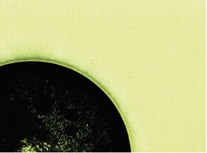
If tape’s adhesive force is too strong, wafers may crack when peeling BG tapes. Therefore, tapes must be easily releasable. Circuits fabricated on silicon wafers have fine irregularities. If BG tapes do not follow these irregularities and bubbles or gaps generate, the grind water that is used when grinding wafers can contaminate circuits. Furthermore, the generation of dimples due to the concentration of stress, may enable cracking and chipping of wafers during grinding. For this reason, BG tapes is essential to have high followability to irregularities of circuit surface.
However, in recent years, wafer-level chip size packages (WLCSPs) have come to be used widely. In WLCSPs, bump electrodes with a height of 200μm or higher mount on circuits formed on the wafer, making it difficult for general-purpose BG tapes to secure followability for these wafers.
Hence, Maxell has developed BG tapes that support these high bumps.
Characteristics of BG Tapes
Low contamination property
Contamination of circuits by the adhesion of BG tapes can occur at the edge of bubbles that generate around bumps. Maxell has suppressed the adhering of adhesives to circuits by using adhesives that do not contain low-molecular weight components.
Easy releasability
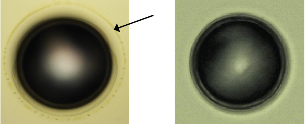
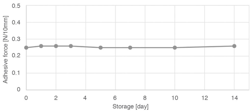
Maxell offers pressure-sensitive type and ultraviolet (UV) release type adhesives. These adhesives peel tapes without damaging thin silicon wafers, leveraging technologies accumulated in dicing tapes. When the initial adhesive force with respect to wafer is low, tapes peel off from the wafer in the back grinding process, and intrusion of grinding water occurs. The company’s adjusted BG tapes exhibit high adhesive force in the initial stage to prevent the intrusion of grinding water, and peel easily at the time of removal (Fig. 3). Also, there will be little change in the peeling force even after attaching the tape on the wafers for a long period, which is one of the major characteristics of Maxell’s BG tapes (Fig. 4).
Followability
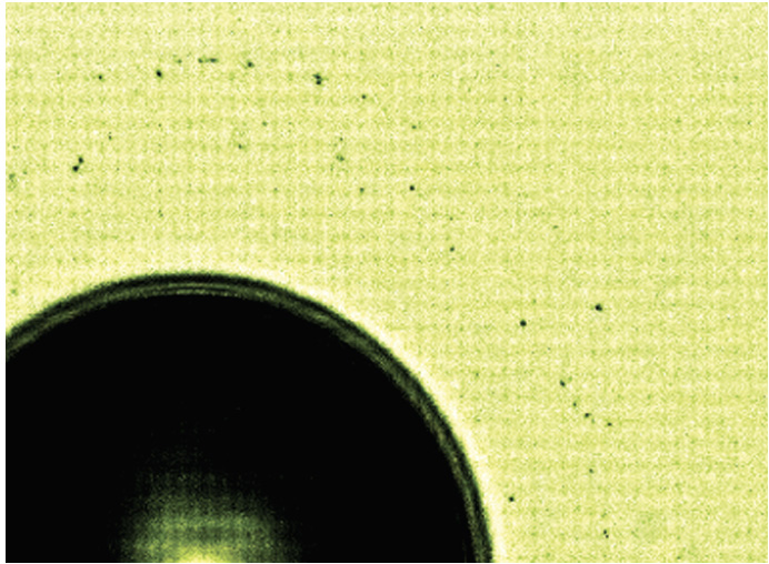
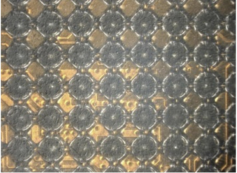
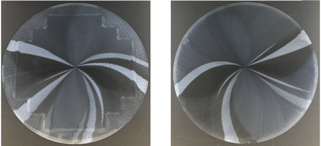
Maxell’s BG tapes have a thermoplastic intermediate layer to be able to sufficiently follow high bumps. When followability to bumps is low, dimples generate on the backside of wafers after back grinding. Maxell’s BG tapes can sufficiently follow bumps by heating the BG tapes when adhered to bumps and soften the intermediate layer. The generation of dimples can also be suppressed (Figs. 5 and 6).
To support various wafers with bumps, Maxell has in its lineup BG tapes with the intermediate layer of various thicknesses, and those with different levels of adhesive force.
With the advancement of the semiconductor fabrication process, BG tapes and other adhesive tapes for semiconductor process will be required to meet various demands.
Maxell will develop technologies to quickly meet these demands and provide products that help solve customers’ issues.
- Share:


About This Article:
The author is Munehiro Morimoto, Manager, No. 3 Design Department, Design Division, Functional Materials Division, Maxell, Ltd.