ASIA ELECTRONICS INDUSTRYYOUR WINDOW TO SMART MANUFACTURING
Record Growth in Chip Equipment to Extend in 2022
Overall, the novel coronavirus (COVID-19) pandemic has made a huge impact in the semiconductor manufacturing equipment supply chain, as it forced governments to impose lockdown measures to control the infection. In turn, manufacturers had to resort to temporary fab closures and production downtime due to shortage in manpower, limited supply and logistics woes. The delay in production further adversely affected the supply of semiconductor chips and ICs.
On a positive note, it is also because of the pandemic that the industry will see record performance this year. The accelerated digital transformation arising from the changes in lifestyles and work schemes is poised to drive the market to new record highs. Specifically, sales of semiconductor manufacturing equipment will top US$95 billion this year and cross US$100 billion in 2020, according to SEMI. Consumer demand for smartphones, computers, data infrastructure, vehicle electrification and advanced industrial applications will collectively drive the demand for cutting-edge semiconductor chips.
US$100 Billion Market
This year, sales of semiconductor manufacturing equipment is projected to reach US$95.3 billion, an impressive annual growth of 34 percent according to SEMI. This outstanding performance will extend to 2022 with an annual sales forecast of US$101.3 billion. These will be driven mainly by sustained capital expenditures by device makers in secular growth for the expansion of front-end and back-end semiconductor equipment segments.
Specifically, the wafer fab equipment segment is projected to surge 34 percent to a new industry record of US$81.7 billion in 2021, followed by a 6 percent increase in 2022 to more than US$86 billion. The wafer fab equipment segment includes wafer processing, fab facilities, and mask/reticle equipment.
Meanwhile, the foundry and logic segments will expand 39 percent annually to US$45.7 billion in 2021 on strong demand for leading-edge technologies powered by the digitization of industries. The growth momentum is expected to continue in 2022 with the foundry and logic equipment investments by another 8 percent growth.
Robust demand for memory and storage is driving spending on NAND and DRAM manufacturing equipment. The DRAM equipment segment is expected to lead the expansion in 2021, surging 46 percent to surpass US$14 billion. The NAND flash equipment market is projected to increase 13 percent in 2021 to US$17.4 billion and in 2022 to US$18.9 billion, respectively.
The assembly and packaging equipment segment is forecast to grow 56 percent to US$6 billion in 2021, followed by a 6 percent increase in 2022, driven by advanced packaging applications. The semiconductor test equipment market is expected to grow 26 percent in 2021 to US$7.6 billion and expand another 6 percent in 2022 on demand for 5G and high-performance computing (HPC) applications.
Meanwhile, GM Insights attributed the potential growth to the growing adoption of advanced packaging techniques from across Integrated Devices Manufacturers (IDMs) and foundries. Advanced packaging technology helps these players to manufacture technically advanced semiconductor wafers and chipsets that offer high performance, a smaller footprint, and low-power consumption features.
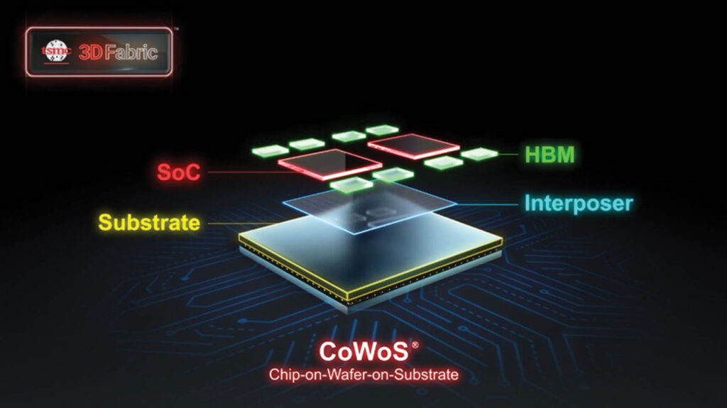
Three-dimensional die stacking technologies can handle thinner wafers and dies to below 30µm. Recently, Taiwan Semiconductor Manufacturing Company Limited (TSMC) announced the 3DFabric family of 3D silicon and advanced packaging technologies (Photo 1). At Computex 2021, Analog Micro Devices, Inc. (AMD) CEO Lisa Su, announced the next-generation Ryzen 9 CPU with vertically stacked static RAM. Advancing these developments further, the Institute of Microelectronics has developed a cutting-edge 3D die stacking technologies allowing four semiconductor layers to be stacked.
Going Back to Normal
This year, with the aggressive vaccination rollouts worldwide, the market situation is expected to go back to normal. According to a report by Allied Market Research, this is expected to lead to re-initiation of semiconductor production equipment companies at their full-scale capacities, which would aid the market to recover by the start of 2022.
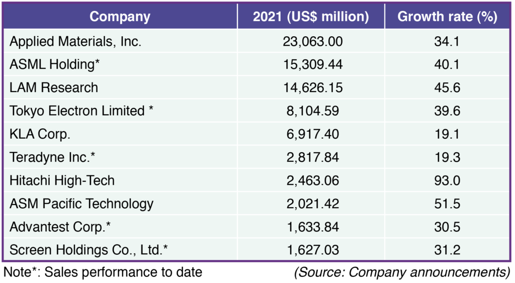
As the market goes back to normal, leading manufacturing equipment vendors saw this trend reflected on their revenue data. Based on their sales performance, double-digit growths were recorded compared to the same period a year ago (Table).
Seeing to benefit from strong demand for semiconductor systems, market leader Applied Materials, Inc. reported 34 percent growth in sales for FY2021 (ending Oct. 2021) to US$23.1 billion, and leads the top 10 semiconductor manufacturing equipment suppliers. “Demand for semiconductors and equipment continues to grow as the pandemic accelerates digital transformation of the economy, and currently, our supply chain cannot keep up,” said Gary Dickerson, President and Chief Executive Officer.
“Overall orders were up by 62 percent year over year and semiconductor systems orders were up 78 percent,” said Bob Halliday, Senior Vice President and Chief Financial Officer. “The momentum continued as our Semiconductor Systems backlog increased during the fourth quarter from US$5.5 billion to US$6.7 billion, and we see this strength sustaining into 2022.”
For ASML, 2021 will be another highlight year. For the first three quarters, it reported EUR13.6 billion (US$15.3 billion) in sales, up by 40 percent. According to ASML President and Chief Executive Officer Peter Wennink, “For 2021, we expect another year of growth driven by strong Logic demand and continued recovery in Memory. The build out of the digital infrastructure and the continued technology innovation is relevant to the consumer, automotive and industrial markets and drives demand across our entire product portfolio,”
Recently, ASML opens new state-of-the-art R&D facility in Silicon Valley. This forms part of its plan to expand the power of computation from lithography to optical metrology and e-beam inspection, as well as machine learning applications (Photo 2).
Meanwhile, ASM Pacific Technology recorded 51.5 percent growth for the first three quarters of the year to HK$15.7 billion (US$2 billion), and is well on its way to achieve 46 percent growth for the full year to US$2.8 billion. It registered 80.3 percent in bookings for the first three quarters.
The Group has reinforced its core competencies via strong industry partnerships with leading global technology companies. In July 2020, it began a collaboration with IBM Research to develop and deliver a suite of integrated solutions for heterogeneous integration applications to facilitate the assembly of complex artificial intelligence (AI) chips. In Jan. 2021, the Group inked a joint agreement with EV Group to co-develop ultra-precise, highly configurable die-to-wafer hybrid bonding solutions that will be crucial for heterogenous integration applications.
These leading-edge partnerships with key technology leaders have helped strengthen the Group’s strong position in semiconductor development, especially as advanced end-market applications including 5G, HPC and AI rapidly proliferate.
Future Market Drivers
For the future, the Allied Market Research report highlighted the effect of car electrification to the continuous surge in demand for semiconductor manufacturing equipment citing the study by International Energy Agency (IEA). According to IEA, in 2019, electric cars accounted for 2.6 percent of global auto sales and about 1 percent of global car stock, which will be accelerated with a growth rate of 40 percent per year. Microcontrollers, high-power modules, discrete components, and other power semiconductors will be in higher demand as a result, driving the market development.
Technological innovations in extreme ultraviolet (EUV) lithography equipment will also drive the market growth. One by one, companies are employing EUV machines for the production of semiconductor. In Feb. 2019, ASML announced the delivery of 18 high-end lithography machines to Taiwan Semiconductor Manufacturing Company for a total of US$2.16 billion.
Applied Materials has made steps to support wiring of advanced logic chips that enables scaling to the 3nm node and beyond. Recently, it the Endura Copper Barrier Seed IMS, an Integrated Materials Solution that combines seven different process technologies in one system under high vacuum: ALD, PVD, CVD, copper reflow, surface treatment, interface engineering and metrology. The solution also includes copper reflow technology that enables void free gap fill in narrow features. Electrical resistance at the via contact interface is reduced by up to 50 percent, improving chip performance and power consumption, and enabling logic scaling to continue to 3nm and beyond
In May 2021, Applied Materials also released Alx, which accelerates the manufacturing and production of new chip technologies. Through its partnership with BE semiconductor Industries N.V, it plans to create proven equipment solution for die-based hybrid bonding with chip-to-chip connecting technology to improve performance design.
According to Allied Market Research, companies are constantly accessible to technical advancements such as the use of laser plasma as a light source in EUV lithography equipment to produce high-quality wavelengths. This will assist foundry providers in lowering maintenance and operational costs. Therefore, such factors are expected to expand the semiconductor production machine industry.
- Share: