ASIA ELECTRONICS INDUSTRYYOUR WINDOW TO SMART MANUFACTURING
Lasertec to Pitch Advance EUV Lithography Systems
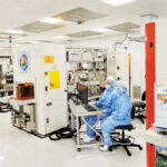
The main products of Lasertec Corporation are the various inspection systems, which support the production of leading-edge semiconductors, allowing the company to contribute to the technological innovations in today’s digital transformation.
With the proliferation of fifth-generation (5G) communication systems and the expansion of data centers, the demand for leading-edge semiconductors has been steadily on the rise. Amongst this, logic and memory device manufacturers are continuing to make active investments. With the onboarding of the cutting-edge semiconductor manufacturing process that utilizes extreme ultraviolet (EUV) lithography accelerating, the demand for Lasertec’s products has continued to expand. With the company receiving a record-breaking ¥108.3 billion (US$ 948 million) of orders in Q1 (July to September) of the fiscal year ending June 2022.
Lasertec Corporation’s Senior Managing Director Koichi Moriizumi, who oversees the company’s sales, is quoted as saying, “We are expecting orders of ¥160 billion (US$1.4 billion) in FY2022 and are making steady progress already achieving 70% of our target orders in Q1. We have noticed a strong trend among manufacturers to invest in the most advanced semiconductors, which will allow our company to continue to advance our business as planned.”

A Robust Demand for EUV-Related Products
As more leading-edge EUV lithography systems come to market, the sales of EUV-related products now account for about 50 percent of the company’s sales. For EUV lithography, Lasertec has commercialized the ACTIS A150 actinic EUV patterned mask inspection system, the first inspection system that uses EUV light, the MATRICS X8ULTRA Series EUV mask inspection system, and the BASIC Series EUV mask backside inspection and cleaning system. The company will showcase its EUV related products at SEMICON Taiwan in December.
Moriizumi says, “The trend of brisk sales of EUV-related products continues in the current fiscal year. Our company continues to enjoy strong demand for our EUV-related products, with both the MATRICS and ACTIS systems, in particular, enjoying a robust demand. So much so that at the end of Q1 the backlog on our products was ¥235 billion (US$2.06 billion).”
The A150 EUV System Adopts Actinic Inspection Technology
The ACTIS A150 is the first EUV patterned mask inspection system to adopt actinic inspection technology, which employs short-wavelength EUV light. The A150 provides an overwhelmingly higher defect detection sensitivity than conventional mask inspection systems that use deep ultra-violet (DUV) lasers, enabling the detection of printable phase defects, an issue unique to EUV masks.
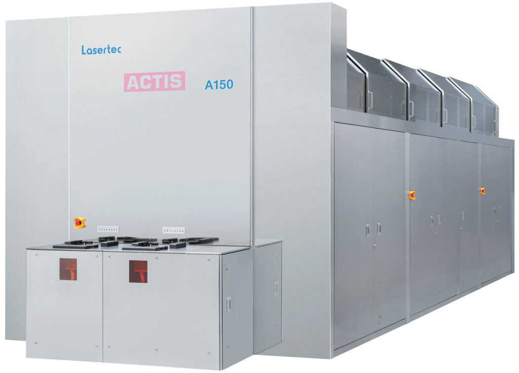
Except for the ACTIS A150, the mask inspection systems available for use in the EUV process rely on the use of DUV. While the DUV lasers on these conventional systems have a wavelength of around 200nm, the EUV light harnessed by A150 has a much shorter wavelength of 13.5nm. This allows the A150 to provide significantly higher resolution and detect defects not detectable by conventional inspection systems.
The use of pellicles in EUV lithography also poses another major issue to conventional inspection systems. A pellicle is a film attached to masks to prevent particles from falling on the pattern surface during the lithography process. The pellicles used in EUV lithography are opaque to DUV light, meaning that mask inspection systems utilizing DUV light cannot inspect EUV masks through their pellicles.
In contrast, the A150 uses EUV light that can pass through the pellicles, enabling the masks to be inspected with the pellicles still attached. By making through-pellicle inspection a reality, the A150 has overcome a significant challenge faced by EUV mask production, contributing to the overall improvement of the EUV lithography wafer yield.
Brisk Sales of Products for Compound Semiconductors
Outside of EUV-related products, Lasertec also enjoys brisk sales of its products for compound semiconductors, including the SICA88 silicon carbide (SiC) wafer inspection and review system. Amid heightened global efforts toward carbon neutrality, the company expects the demand for SiC wafers to expand rapidly.
By offering products that aid in the production of compound semiconductors, Lasertec helps propel advancements in the electrification of automobiles, helping achieve the goal of creating an environmentally friendly society.
Playing its Part in Chip Innovations
Moriizumi says, “Leading-edge semiconductors will continue to get smaller, with the industry setting its sights on 3 to 2nm nodes, and even smaller nodes down the line, and we will continue to develop products based on this road map. The numerical aperture of optical systems will also increase from the current 0.33 to 0.55. We plan to continue advancing our product development, allowing our products to keep pace with the progress of their respective technologies. In FY2022, we plan to invest ¥7.5 billion (US$65.7 million) into R&D and will continue our contributions to the technological innovations of cutting-edge semiconductors.”
- Share: