ASIA ELECTRONICS INDUSTRYYOUR WINDOW TO SMART MANUFACTURING
Nepes Starts Mass-Production of FOPLP Chip-Packaging Line
Nepes Laweh, an advanced 3D chip-packaging unit of Nepes Co., Ltd. of Korea is betting on a boom cycle of SoCs, as it has begun mass-production of FOPLP, a next generation of fan out panel-level packaging that uses 600m x 600mm panel substrates to pack chip dies.
The company said on Dec.7 that its FOPLP chip packaging line has started a full-scale mass-production after it got certified by various customers in the third quarter. The yield – the ratio of marketable versus total production – also proves good enough to start mass production.
The mass-production will enable the chip-packaging company to double its production capacity in 2022, as Nepes’ FOPLP chip-packaging technology boasts of 5.1 times higher productivity in theory than a 300mm WLP, or wafer level package. The mass production facility comes online at a time when supply for chips is still running short.
At the ceremony held on Dec. 7 at its Cheonan FOPLL facility to celebrate the start of mass-production system, Chung, Chil-Hee, chairman of Nepes and GM of Semiconductor Business, said, “”FOPLP is the best packaging solution ever for high-end semiconductors. Our leadership in the technology is the result of our long-term cooperation with global partners such as materials, parts, and equipment.”
FOPLP for Heterogeneous Integration Chip Solutions
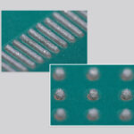
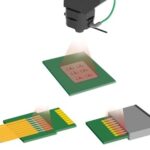
FOPLP technology is a sort of PCB-based chip packaging process technology that punches die-sized holes through PCB substrates called as panels and insert and mold chip dies into the holes. Then, thin film RDL or redistribution layers and solder balls are adhered to the bottom of the panels to be interfaced with other parts and components.
Then, the die-packed panels are diced into individual chip dies.
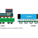
The advantages of FOPLP technology over FOWLP, or fan out wafer level package is higher space utilization, under which more chip dies can be inserted into a panel, as the rectangular shape of the panel can accommodate more chip dies than wafer. On top of that, panel sizes can be easily increased from 400mm x 500mm to 600mm x 600mm. On the contrary, wafer sizes still stay 300 mm in circular shapes, which can utilize less space than the rectangular shape.
The higher space utilization translates into higher productivity and lower costs. The FOPLP is a perfect chip packaging platform for heterogenous chip integration technology, as more and more chips of different functions and designs are integrated on a package level in what’ called as SiP or system in package.
FOPLP Cheonan Campus Sprawls on 186,000㎡ Land Lot
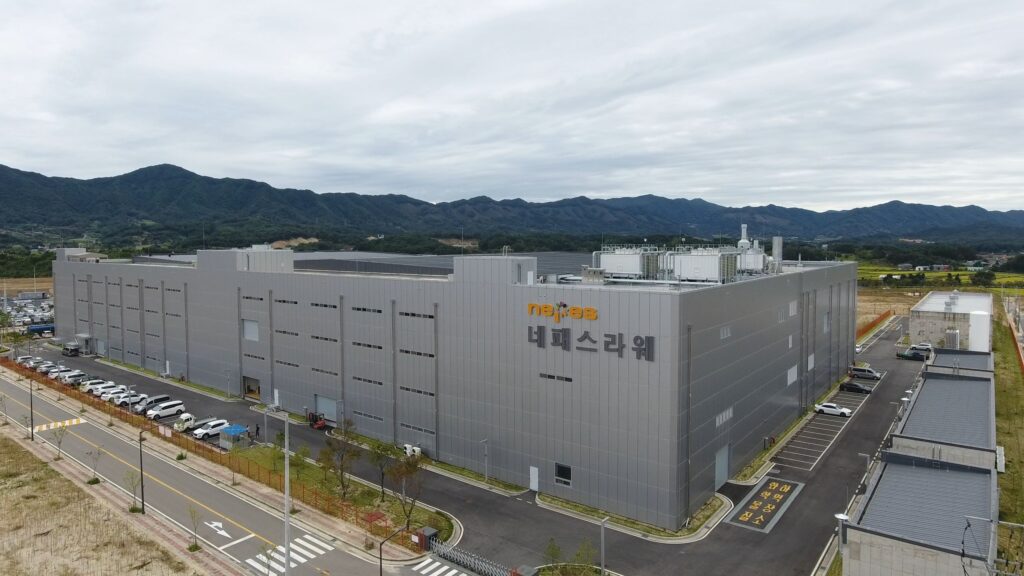
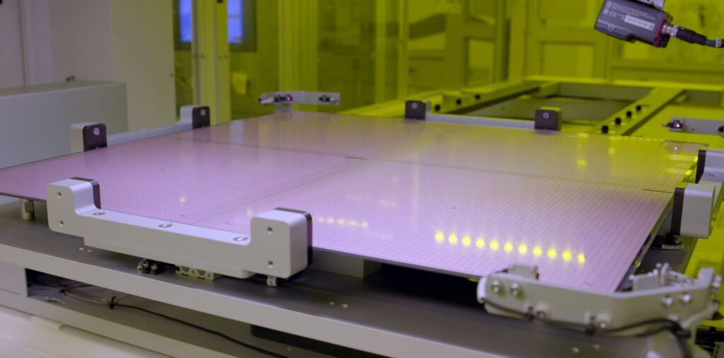
Nepes’ FOPLP production facility is spread across a massive land lot of 186,000㎡ Cheongan Campus located at Cheonan City, a 2 and half an hour-drive south of capital Seoul. The land lot is the equivalent of 25 soccer fields combined in size. Occupying a total building area of 34,000㎡, the fab facilities can produce up to 96,000 panels per year based on 600mm PLP.
According to Nepes, the 600mmx 600mm panel is the largest ever of its kind commercially available now.
Nepes expects demand for FOPLP to explode in the foreseeable future, as demand for SiP and heterogeneous chip solution technologies are also booming to keep up with the rapid proliferation of IoT and 5G, AI, AR and VR applications.
Nepes Laweh is a leading company in the system semiconductor industry with advanced fan-out packaging solution. In the era of the 4th industrial revolution, when high-end and heterogeneous SoCs are in high demand to support 5G, self-driving cars, and Metaverse, Nepes expects its FOPLP chip packaging technology to become new standards for high-end and advanced 3D chip-packaging solutions.
- Share: