ASIA ELECTRONICS INDUSTRYYOUR WINDOW TO SMART MANUFACTURING
ETRI of Korea Commercializes Low-Temperature Photoresist for OLED
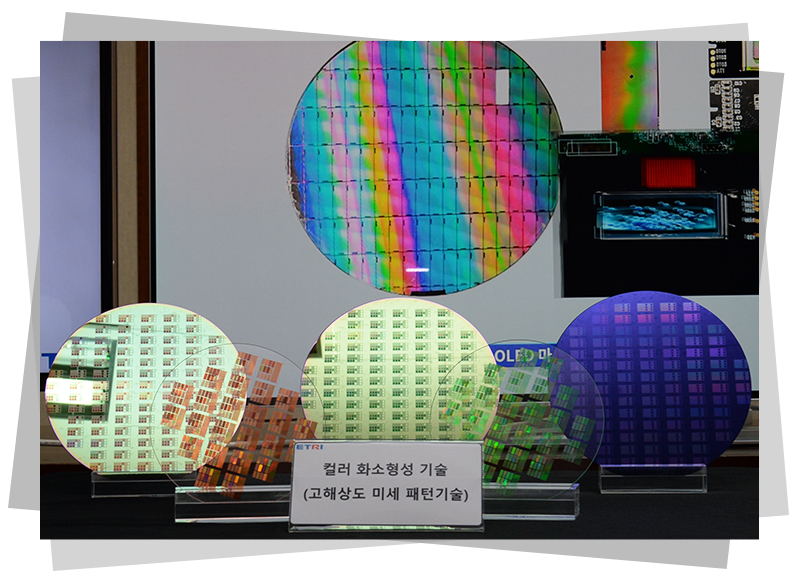
A domestic research team at Korea’s state-funded ETRI has successfully commercialized a material process technology that can concoct photo-resist material at a low temperature.
The photo-resist is a key raw material in forming fine pixels in the OLED display manufacturing process, as it serves as a sort of separator films called as PDL or pixel define layer, which is situated between anode and cathode poles of the pixel.
The PDL takes advantages of the nature of the photo-resist materials, which is changing its property when exposed to light, to define pixel operations.
The technology is now being used to form LED pixels of micro-OLED panels, which are composed of emissive electroluminescence layers, a file of organic compound.

ETRI, or the Electronics and Telecommunications Research Institute, said that the newly formed photoresist process technology has allowed it to create a pixel size of less than 3μm even at the manufacturing temperature of 100℃ or less.
The prototype made by the research team is 0.7inch micro-display which is suitable for wearable devices.
The size of each pixel is 3μm, or thinner and 2,300 pixels per inch are densely populated, so that ultra-high-resolution panels can be produced.
The technology already had secured a use case in a small-sized OLED screen for a smart phone model that was released in 2021 by a Korean company, which wants not to be identified.
Dr. Nam Sung Cho said, “We succeeded in localizing source materials through a national project together with the government, companies, and national research institutes. We hope that this achievement will be helpful for Korea to maintain its status as a leader in the display industry as well as the independence of materials, parts, and equipment.”
ETRI is going to conduct follow-up researches to develop a panel with higher resolutions, aiming to cram 3,000 pixels can fit in 1 inch, and it will continue the discussion on transferring the developed micro-display technology to related companies.


