ASIA ELECTRONICS INDUSTRYYOUR WINDOW TO SMART MANUFACTURING
Lasertec Sees Fresh Market Opportunities in Rapid Adoption of EUV Equipment
Disruptive technologies necessarily call for discontinuous innovations in its old manufacturing ecosystem, presenting new market opportunities for innovators.
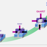
EUV, or extreme ultra-violet photolithography equipment is that case, using high-power source and high-absorption EUV as light source to pattern chip circuitry on a silicon wafer, which is a dramatic departure from predecessor deep ultra-violet lithography technology. So, the semiconductor industry’s ramp up to EUV lithography technology requires disruptive innovations in all of its parts and components ecosystem like PR or photo resist, pellicles, optical lenses, and photomasks, or reticles.
Of particular, the commercial rollout of pellicles, a transparent protector of photomasks against particle contamination, has been challenging, as the protective transparent membrane has to be thin enough and transmissive enough to filter through as much lights as possible.
For example, ASML, a sole EUV equipment maker has been trying to produce high power source and high transmission pellicles, of which light transmittance is over 90%, but with little success.
So, chip makers like Samsung Electronics have no alternative but to carry pellicle-less patterned photomasks to its EUV lithography lines and then pattern and draw chip circuitry pitches on a silicon wafer through the patterned masks, leaving the photomasks very vulnerable to particle and dust contamination and so risking to take lower-than-expected yield.
Vulnerable to Tin Droplet Contamination
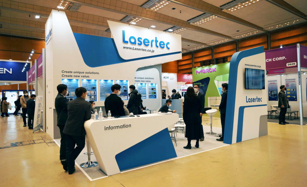
Lasertec of Japan, a maker of laser-based inspection equipment for photomasks and wafers, is one of the innovators that are seeing new market opportunities in the technology disruption.
The semiconductor equipment maker has been finding itself awash in a flood of orders for its EUV photomask inspection systems, as chip makers like Samsung Electronics has been ordering the machines in volume to minimize yield losses, which occurs at its EUV lithography lines.
“It is no coincident that demand for our EUV photomask inspection system has been soaring. As high-transmissive EUV photomask pellicles are not available so far, chip makers are more turning to a photomask inspection system to minimize yield losses. We have supplied our Matrics X8Ultra series of photomask inspection system in high volume in Taiwan, U.S., and Korea, said Lim Choon-Gab, director of sales group with Lasertec.
“Looking forward, we expect our brand-new Actis A150 series of EUV patterned mask inspection system to drive up sales in 2022 and beyond, because investments on EUV equipment will continue. The series are the world’s first EUV patterned mask inspection system. We have already secured orders from major chipmakers that are running EUV lines,” he continued.
Die-to-Die Inspection
Photomasks, or often called as reticles, are a sort of master templates where EDA-drawn chip design layouts files are electronically transferred. The photolithography process is to shine EUV lights through the patterned masks to draw fine pitches of chip circuitry on a silicon wafer. The photomasks are susceptible to particle and dust contamination from mask pattering all the way through wafer patterning, and so protective cover pellicles are an indispensable part in the lithography processes.
When it comes to EUV masks, they are more vulnerable to impurity contaminations because EUV light source is a laser-driven tin plasma. So, the photomask is susceptible to tin droplets.
Lasertec’s Actis 150 series of patterned photomask inspection system is the latest of its photo mask inspection system that use laser lights to do actinic inspection to detect and identify printable defects on EUV masks. The actinic inspection also has an ability not only to detect phase defects inside multilayer of EUV masks, but also inspect through-pellicle EUV masks.
Die-to-die and die-to-database inspection is available too.
Director Lim expects Actis A150 series and Matrics X8Ultra series both would boost sales even in 2022, as the adoption of EUV equipment will speed up.
True enough, for example, SK hynix will start phase 2 construction project of its EUV-based M16 wafer fabrication facility this year.
Samsung is also speeding its construction projects to build its P3 EUV wafer fabrication facility that will operate as a hybrid facility for memory chips and foundry services in late 2022. The world’s largest is slated to break ground its P4 EUV facility in 2022 while it will start construction of a Taylor, Texas, U.S.-based EUV fab facility in 2023.
- Share: