ASIA ELECTRONICS INDUSTRYYOUR WINDOW TO SMART MANUFACTURING
Samsung's Ramp-up to 3D GAA Logic Chip Gains Speed on Lam Research's Breakthrough Tools
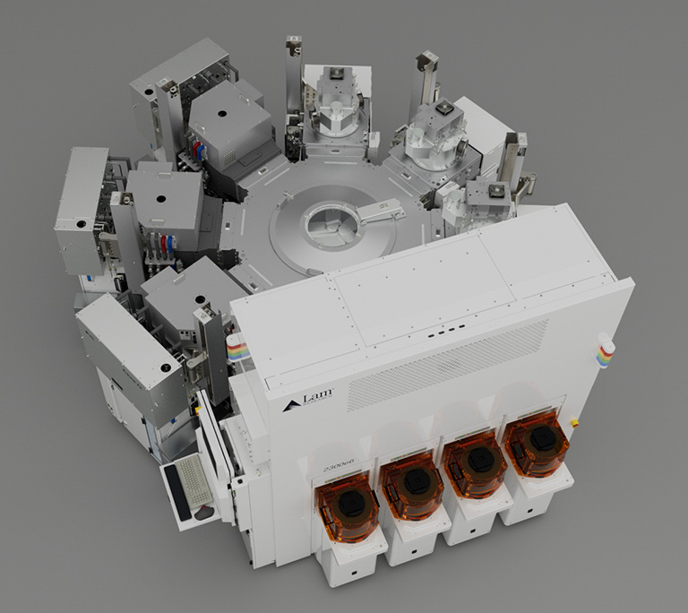
Global semiconductor etching equipment giant Lam Research has rolled out a brand-new series of selective etchers in what the equipment maker said is the must-have breakthrough in the industry’s ramp up to vertically-stacked 3D transistor structure.
The technology breakthrough comes at a time when chip makers like Samsung Electronics is charting out a roadmap to transform DRAM transistor structure from conventional planar type to 3D shape.
At a keynote speech for Semicon 2022 held in Seoul from Feb 9 to 11, research head of Samsung Electronics has introduced a new type of vertical transistor DRAM cells in what’s called as vertical channel access transistor, VCAT.
The ground-breaking selective etching technology also makes public just a couple of months before Samsung Electronics plans to roll out its 3nm GAA, or gate-around-around 3D logic chips sometime in the first half of 2022.
The selective etcher allows chip makers to etch out materials from wafer surface selectively and isotropically or uniformly in all directions with no damages to other critical material layers.
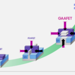
So, this breakthrough helps chip makers to vertically stack transistors, as logic chip maker are struggling to commercialize GAA or nano-sheet 3D logic transistors.
3nm GAA Logic Chips: Just Around Corner
But also, it will allow even DRAM chip makers to transform DRAM transistor cells structures from planar to 3D, following the commercial rollout of 3D NAND flash memory chips.
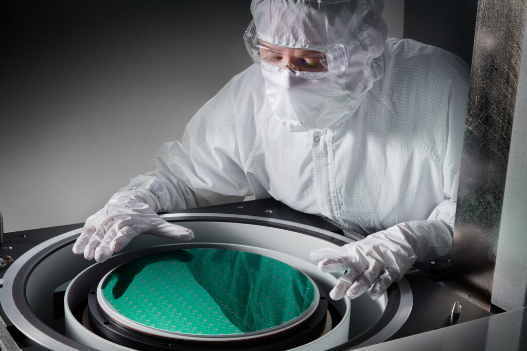
Etching process is to etch out materials from a silicon wafer. In chip-fabrication processes, etching processes are done usually in many steps. The most crucial step is to selectively etch out or remove light-exposed materials from PR-coated wafer surface after the photolithography process is done.
“Developed in collaboration with the world’s most innovative logic and foundry chipmakers, the selective etch products are already being used in the fabs of industry leaders like Samsung Electronics,” Lam Research said in its statement.
“The semiconductor industry is continuously driven toward more powerful and faster device capability. As the density and complexity of the devices have been increasing significantly, selective etch technology is critical to manufacturing our most advanced logic device,” said Dr. Keun Hee Bai, Master of Semiconductor R&D Center at Samsung. “As global demand for Samsung’s technologies continues to soar, we rely on the extensive innovation and capabilities of selective etch to bolster production and accelerate our logic device roadmap toward advanced logic GAA and beyond.”
Samsung Electronics, for example, is now developing a 3nm GAA logic chips using a nanosheet-based multi-channel bridge FET or MCBFET to break through scaling limits of FinFET technology.
Its roadmap calls for the first version of the nanosheet-based 3nano GAA logic chips to roll off the line in the first half of 2022.
Trailblazer to 3D DRAM Transistor Cells
The second version of the 3nm GAA logic chips is scheduled to roll off the line in 2023 and then by 2025, Samsung aims to churn out a 2nm GAA logic chip.
To support Samsung’s roadmap, Lam Research Korea, a Korean subsidiary of Lam Research has been producing the selective etching tools. Lam Research is operating three manufacturing facilities in Korea.
The selective etching tool portfolio include Argos Prevos, and Selis products.
The Argos come with revolutionary MARS , or Metastable Activated Radical Source technology, selectively modifying and decontaminating wafer surfaces. Its groundbreaking treatment and conditioning capabilities enable chipmakers to treat wafer surfaces precisely, optimizing them for peak performance.
The Prevos enables atomic layer precision, ultra-high selectivity etching for oxide, silicon, and metal by combining novel chemistries and innovative vapor technology with agile temperature control.
Prevos leverages a new proprietary chemical technology solution developed by Lam; additional chemistries can be added to support chipmakers’ production needs.
Selis uniquely employs both radical and thermal etch capabilities to enable ultra-high selective etching with uniform top to bottom process control without causing damage to the wafer structure.
Prevos and Selis can also be delivered as a single, integrated tool to provide unique multi-layer selective etching, improved queue-time control, and maximum production flexibility.
“Lam Research is driving the wafer fabrication advancements needed to support the chip industry’s move to 3D architectures and make the next generation of digital technologies a reality,” said Tim Archer, president and chief executive officer at Lam Research. “For more than 40 years, Lam has led the industry in etch innovation. We are proud to continue that tradition with the delivery of the most cutting-edge suite of selective etch solutions for advanced logic and memory available in the market today.”
- Share: