ASIA ELECTRONICS INDUSTRYYOUR WINDOW TO SMART MANUFACTURING
CyberOptics’ New Technologies Improve Fab Yield Time
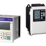
Developer and manufacturer of high-precision 3D sensing technology solutions CyberOptics Corporation will introduce its next-generation lineup of automated sensors for wafers. Particularly, the new portfolio are the WaferSense Auto Teaching System (ATS2) and new ReticleSense Auto Teaching System (ATSR).
Meet Wafer Fab Needs
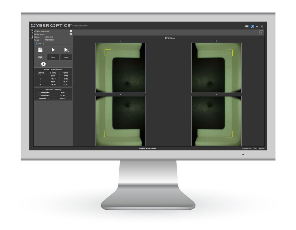
To illustrate, the ATS2 and ATSR are multi camera sensors that work together with CyberOptics’ CyberSpectrum software. In other words, these combo of sensors and software teach accurate wafer and reticle hand-off calibration for proper alignment and set-up of semiconductor tools.
Most importantly, the sensors “see” inside to capture three dimensional (3D) off-set data (x, y, and z) in real-time to quickly teach wafer and reticle transfer positions. All these without opening the tools. Process and equipment engineers can conduct repeatable and reproducible setups and maintenance checks, speed troubleshooting and eliminate technician-to-technician variation.
Dr. Subodh Kulkarni, President, and CEO at CyberOptics said semiconductor fabs around the world recognize their teaching sensors as the most efficient and effective wireless devices for wafer had-off teaching.
“We have advanced the technology to enable even better performance, with the combination of accuracy, precision and versatility that fabs rely on to significantly improve their yields and tool uptime.”
Overview, Features
The ATS improves yields and lower particulate contamination with accurate wafer handoff calibration. In addition, it also achieves repeatable and reproducible semiconductor equipment setups. It also reduces equipment downtime from hours to just minutes. Furthermore, ATS also offers speed trouble-shooting and lower consumable expense with visual inspection.
Meanwhile, the ATSR quickly teaches accurate wafer and reticle hand-off calibration for proper alignment and set-up of semiconductor tools. Without the need of opening the tools, the ATSR sees inside the tools to capture 3D off-set data in real time. Thus, quickly teaching wafer and reticle transfer positions. In addition, it also conducts repeatable and reproducible setups and maintenance checks, speed troubleshooting. At the same time, it also eliminates technician-to-technician variation.
CyberOptics will highlight these two next-generation solutions at the forthcoming SEMICON West 2022 HYBRID. This will take place from July 12 to 14 at Moscone Center in San Francisco, California. Moreover, the company will also demonstrate its WaferSense sensors for leveling, vibration, gapping, relative humidity, resistance, and airborne particles.
- Share: