ASIA ELECTRONICS INDUSTRYYOUR WINDOW TO SMART MANUFACTURING
TSMC’s New Center Tracks Potentials of 3DIC
The pace of microfabrication that has achieved higher performance of semiconductors has begun to slow down. Simultaneously, technological development of three-dimensional (3D) silicon stacking has been gathering steam.
Here, the technology stacks chips in the vertical direction to improve semiconductor performance. Taiwan Semiconductor Manufacturing Company (TSMC) and U.S.-based Intel Corporation have led the front-end process field of logic semiconductor chips. Now, they have expanded investments and are vying in the development of integration technologies and advanced packaging technologies.

Sophisticated Packaging Technology
Recently, two-dimensional (2D) packaging technology called “chiplet” has been attracting attention. Chips (chiplets) produced using optimum process nodes and equipment for CPUs, GPUs and SRAMs are combined like blocks. Then, the combined chiplets appear on a single interposer and housed in a single package using system-on-package (SoP) technology. Thus, the technology achieves miniaturization and functional enhancement of semiconductors without depending on microfabrication.
Furthermore, the technology reduces each chiplet’s size, leading to improved yield, and shorter period to market introduction.
Advanced Micro Devices (AMD) has adopted this technology in Ryzen CPUs for PCs and EPYC processors for servers early on. These AMD processors surpass rival processors in terms of performance, such as those from Intel that adopt monolithic dies. Thus, they have provided an opportunity for AMD to leap forward. Thereafter, AMD has also developed 3D chiplet, wherein SRAMs are stacked on a CPU die in the vertical direction, thereby significantly improving the performance of CPUs.
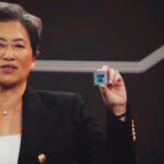
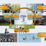
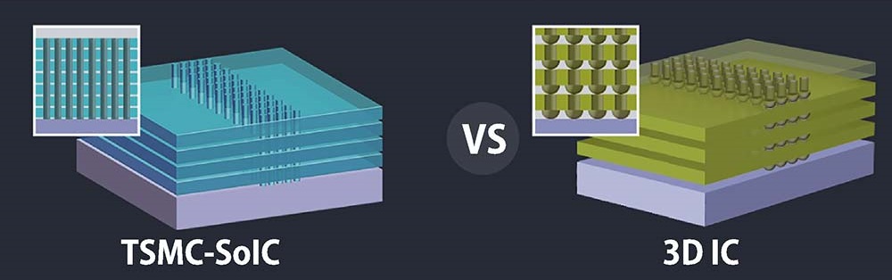
TSMC manufactures AMD’s chips. TSMC is a leader in the front-end process of semiconductor manufacturing. However, it has also been focusing on packaging technologies over many years. Nonetheless, the company provides Chip on Wafer on Substrate (CoWoS) 2D packaging technology and Integrated Fan-Out (InFO) technology. Furthermore, the company has also developed System on Integrated Chips (SoIC) 3D packaging technology to combine with these technologies (Figure).
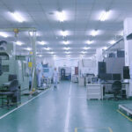
In June, TSMC opened TSMC Japan 3DIC R&D Center, facilities for the research of 2D and 3D packaging technologies. Located in Tsukuba in Japan’s Ibaraki Prefecture, this is TSMC’s first research facilities established outside Taiwan.
Eyes Performance Enhancement of ICs
In his address at the opening ceremony, Yutaka Emoto, Center General Manager, said, “Manufacturers of materials, such as substrates, and manufacturing equipment manufacturers concentrate in Japan. This enables us to speedily exchange information with those manufacturers as we conduct research.” He explained advantages of having research facilities in Japan.
TSMC Japan 3DIC R&D Center is a project under the sponsorship of the Japanese government aimed at achieving the resurgence of the country’s semiconductor industry. It also attracts high attention of the world. Specifically, it provides major business opportunities for Japan’s materials and equipment manufacturers.
Intel and Korea’s Samsung Electronics Co., Ltd. also work earnestly on packaging technologies. Intel has high-density packaging technologies, such as EMIB and Foveros. Earlier last year, the company has expanded investments in Rio Rancho facilities in New Mexico and Malaysian plant to strengthen packaging. The company also plans to establish facilities for packaging in Europe as well.
Leadership race in advanced semiconductors has been becoming increasingly intensified. Under these circumstances, industry-leading companies mention in unison the importance of collaborations with partner companies.
Regarding chiplets, an industry organization that promotes an open standard, UCIe1.0, emerged in May to establish interconnect among chiplets. UCIe™ stands for Universal Chiplet Interconnect Express.
Leading packaging manufacturers, including Taiwan-based Advanced Semiconductor Engineering, Inc. (ASE), AMD, Intel, Samsung Electronics, and TSMC, as well as leading U.S IT companies, such as Microsoft Corporation, take part in the organization. These promoter-members foster widespread use of chipsets beyond the boundaries of companies and accelerate the performance enhancement of semiconductors. Japanese companies with strengths in materials will likely play an important role to combine and integrate technologies of these companies.
- Share: