ASIA ELECTRONICS INDUSTRYYOUR WINDOW TO SMART MANUFACTURING
Demand Surge to Aim IC Fab Constructs to New Heights
The rapid digitalization and emergence of megatrends across industries have brought an unprecedented surge in semiconductor demand. Moreover, recent global events, including geopolitical tensions, have highlighted the need for manufacturers to establish a solid chip supply chain back home.
For that reason, several chipmakers have already started or about to begin new fab construction to meet the demand growth. Ajit Manocha, SEMI President and CEO, said, “Generative AI and high-performance computing are fueling advancements in the leading-edge logic and memory segments, while mainstream nodes continue to underpin critical applications in automotive, IoT and power electronics. The construction of 18 new semiconductor fabs set to begin in 2025 demonstrates the industry’s commitment to support innovation and significant economic growth.”
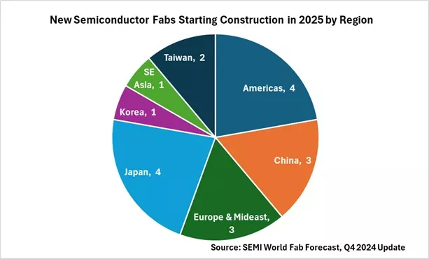
SEMI, in its recent World Fab Forecast report, said of the 18 new fab construction projects in 2025, the Americas and Japan are leading having four each. The China and Europe & Middle East regions are each tied for third place with three planned construction projects. Taiwan has two planned projects, while Korea and Southeast Asia have one project each for 2025.
The SEMI report also mentioned chip capacity is projected to further accelerate, with a 6.6% yearly growth rate forecast to total 33.6 million wafers per month (wpm) for 2025. This expansion will be primarily driven by leading-edge logic technologies in high-performance computing (HPC) applications and the increasing penetration of generative AI in edge devices.
New Fab Projects
Major foundry players that have announced new fab constructions early on would soon start to operate their fabs from this year onwards.
Hua Hong Semiconductor Limited
Leading Chinese pure-play foundry Hua Hong Semiconductor has an ongoing construction for a new 12-inch IC production line, the Hua Hong Manufacturing. The project is located inside the Hua Hong Wuxi Phase-II project.
Currently, the company already has a 12-inch production line devoted to specialty processes and is currently the world’s first 12-inch power semiconductor foundry. Moreover, the company also has existing three 8-inch wafer fab facilities in Shanghai Jinqiao and Shanghai Zhangjiang, which have monthly 8-inch capacity of approximately 180,000 wafers.
Intel Corporation
Intel is set to start producing its US$20-billion 300mm fab soon in New Albany in Ohio, United States. The New Albany site, which includes two chip factories, has an initial aggressive production goal of 2025. However, recent announcements by the company, citing changes in pacing of construction, might see the actual production date at around 2026.
The new fabs are part of a reset of Intel’s manufacturing, a plan called IDM 2.0, that would see Intel regain its ability to make chips at the most advanced nodes and offer foundry services to other companies. It also comes as the United States embarks on an effort to grow advanced chipmaking capacity.
Kioxia Corporation
Japanese NAND flash giant Kioxia Corporation will soon start the operation of its new 300mm wafer fab for its proprietary 3D flash memory BiCS FLASH™ at the Kitakami Plant. As demand is recovering, the company will gradually make capital investments while closely monitoring flash memory market trends. Kioxia plans to start operation at K2 in the fall of Calendar Year 2025.
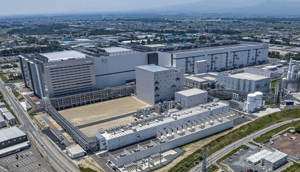
A portion of the investment for K2 will be subsidized by the Japanese government according to the plan approved in February 2024. In addition, some administration and engineering departments will move into a new administration building located adjacent to K2 beginning in November 2024 to oversee the operation of K2.
Micron Technology, Inc.
Micron Technology, Inc.’s initial investment of US$15 billion for a new fab for leading-edge memory manufacturing in Boise, Idaho is expected to start its production in phases this year. The said investment is part of the company’s US$120 billion cumulative investments for the next 20 years to build leading-edge memory manufacturing and R&Ds in multiple phases in the United States.
The said Micron investments also earned US$6.1 billion funding support under the CHIPS and Science Act of the U.S. government. The construction of the new fab in Boise started in early 2023, with cleanroom space coming online in phases starting in 2025.
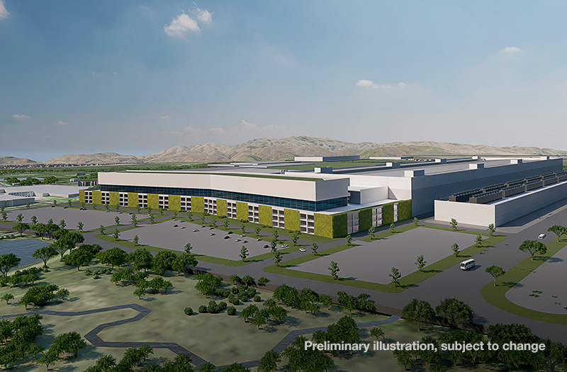
New DRAM production is targeted to start in 2025, ramping over the second half of the decade in line with industry demand growth. Ultimately, the cleanroom space will reach 600,000 square feet — the size of approximately 10 U.S. football fields and the largest single cleanroom ever built in the country.
Samsung
Samsung Electronics has also announced in 2022 plans to expand its Pyeontaek line in Korea, with the goal of starting mass production in June this year. Although not much details were known officially from the company, market intelligence company Trendforce said in August 2024 that the Pyeontaek plant 4 (P4) was supposed to have four phases to focus on 6th generation DRAM production line. The construction was supposedly facing some delays amid downscaled demand.
Rapidus Corporation
Japan’s Rapidus Corporation is currently building a new 2nm semiconductor plant, the Innovative Integration for Manufacturing (IIM-1) inside Chitose City in Hokkaido.
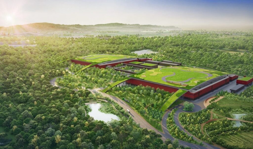
The facility will be Japan’s first to produce state-of-the-art logic semiconductors at 2nm and beyond. Targeted to start operations in 2025, the new facility will likely begin mass production in 2027.
TSMC
Taiwan Semiconductor Manufacturing Company Ltd. (TSMC) is building two semiconductor fabs in Arizona, United States, tripling its investments from the original US$12 billion to US$40 billion.
The first fab was supposedly due for completion in 2024 while the second fab was due in 2026. However, the company recently said that the first fab would not start operating until 2025. When the two fabs become operational, TSMC expects to manufacture over 600,000 wafers per year.
Advanced Nodes Lead Expansion
The SEMI report also said the chip industry is intensifying efforts to build advanced computing capabilities, responding to the escalating computational demands of large language models (LLMs). Chip manufacturers are aggressively expanding advanced node capacities (7nm and below), which are expected to see an industry-leading 16% yearly growth rate for an increase of more than 300,000 wpm to total 2.2 million wpm in 2025.
Boosted by China’s chip self-sufficiency strategy and expected demand from automotive and IoT applications, mainstream nodes (8nm~45nm) are predicted to add another 6% capacity, surpassing the 15 million wpm milestone in 2025.
Mature technology nodes (50nm and above) are experiencing a more conservative expansion, reflecting the market’s slow recovery and low utilization rates. This segment is expected to grow 5%, reaching 14 million wpm in 2025.Spanning 2023 to 2025, the SEMI report said. About 97 new high volume fabs are about to begin operations, about 48 projects happened in in 2024 and about 32 more will happen in 2025, with wafer sizes ranging from 300mm to 50mm.
The Foundry segment is projected to increase capacity by 10.9% year-over-year, rising from 11.3 million wpm in 2024 to a record 12.6 million wpm in 2025.
The overall memory segment shows a measured capacity expansion, with modest growth of 3.5% in 2024 and 2.9% in 2025. However, strong generative AI demand is driving significant changes in memory markets. High-bandwidth memory (HBM) is experiencing a notable surge, creating divergent capacity growth trends between the DRAM and NAND flash segments.
The DRAM segment is expected to maintain robust growth, projecting approximately a 7% year-over-year increase to 4.5 million wpm in 2025. Conversely, the installed capacity for 3D NAND is anticipated to grow 5%, reaching 3.7 million wpm in the same period.
17 January 2024

