ASIA ELECTRONICS INDUSTRYYOUR WINDOW TO SMART MANUFACTURING
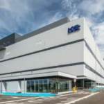
New Center to Lift Kokusai Electric's U.S. Market Grit
KOKUSAI ELECTRIC will soon establish a new new demo center in Oregon, United States. Specifically, the new center will aim to strengthen its demo evaluation function and support system for U.S. semiconductor device manufacturers.
Aiming to start operation in September 2026, the center will accelerate the development of semiconductor manufacturing technologies that are becoming increasingly complex.
Background of New Center
The semiconductor device market is expanding rapidly due to the growing demand for electronic devices such as smartphones and computers, the expansion of data centers driven by the spread of technologies including 5G, AI, IoT, and DX. Add to these are the increasing industrial demand for investments in measures such as reducing environmental impact (GX) and industrial support measures by major countries.
Furthermore, as cutting-edge semiconductor device structures become more complex, three-dimensional, and miniaturized, semiconductor device manufacturers are increasingly requesting our group to provide development support through demo evaluations and other methods.
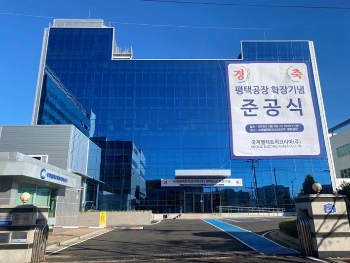
In this market environment, our group is strengthening its efforts to provide development support in response to customer requests by expanding its demo evaluation area to the Pyeongtaek Factory of our group company, Kook Je Electric Korea Co., Ltd. in South Korea. As part of the company’s efforts to strengthen its customer development support system, the company has decided to establish a new U.S. Demo Center in Oregon, United States.
Enhances Local Support System
The new center will enable Kokusai Electric to quickly complete demo evaluations for U.S. semiconductor device manufacturers, which have previously been conducted at the Toyama Technology & Manufacturing Center. This will result in cost efficiency and it is not necessary to transport evaluation wafers and personnel between Japan and the United States.
Additionally, by enhancing its local support system, the company will be able to accurately ascertain our customers’ issues. Thus, allowing us to provide more meticulous support for their research and development efforts. “We envision expansion of the U.S. Demo Center in response to future demand trends, with the aim of further strengthening our customer development support system,” said Kokusai Electric.
The new US Demo Center will have a site area of approximately 34,000sq.m and will be a one-story building. Construction is scheduled to begin in September of this year, with completion scheduled for September 2026. The investment amount is expected to be approximately 20 billion yen.
Currently, the semiconductor device market is polarized, with demand for cutting-edge semiconductor devices related to AI and other areas being high, while demand for in-vehicle, PC, and smartphone devices is sluggish. In addition, the structure of cutting-edge semiconductor devices is becoming more complex every year, and there are increasing requests from semiconductor device manufacturers for development support through demo evaluations, etc.
14 April 2025
- Share: