ASIA ELECTRONICS INDUSTRYYOUR WINDOW TO SMART MANUFACTURING
Applied Materials’ New Tools to Edge Better AI Chips
Applied Materials, Inc. has unveiled its latest semiconductor manufacturing systems that will enable advanced logic and memory chips to suit artificial intelligence (AI) computing.
The next-generation chipmaking tools target three critical fields to deliver powerful AI chips. These are leading-edge logic including Gate-All-Around (GAA) transistors, high-performance DRAM including high-bandwidth memory (HBM), and advanced packaging. Therefore, creating a highly integrated systems-in-a-package that optimize chip performance, power consumption and cost.
Dr. Prabu Raja, President of the Semiconductor Products Group at Applied Materials said the company is focusing on driving materials engineering breakthroughs to provide improvements needed to scale AI. “We are collaborating earlier and deeper with our customers to co-develop solutions that accelerate chipmaker roadmaps and enable major device inflections in logic, memory and advanced packaging.”
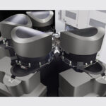
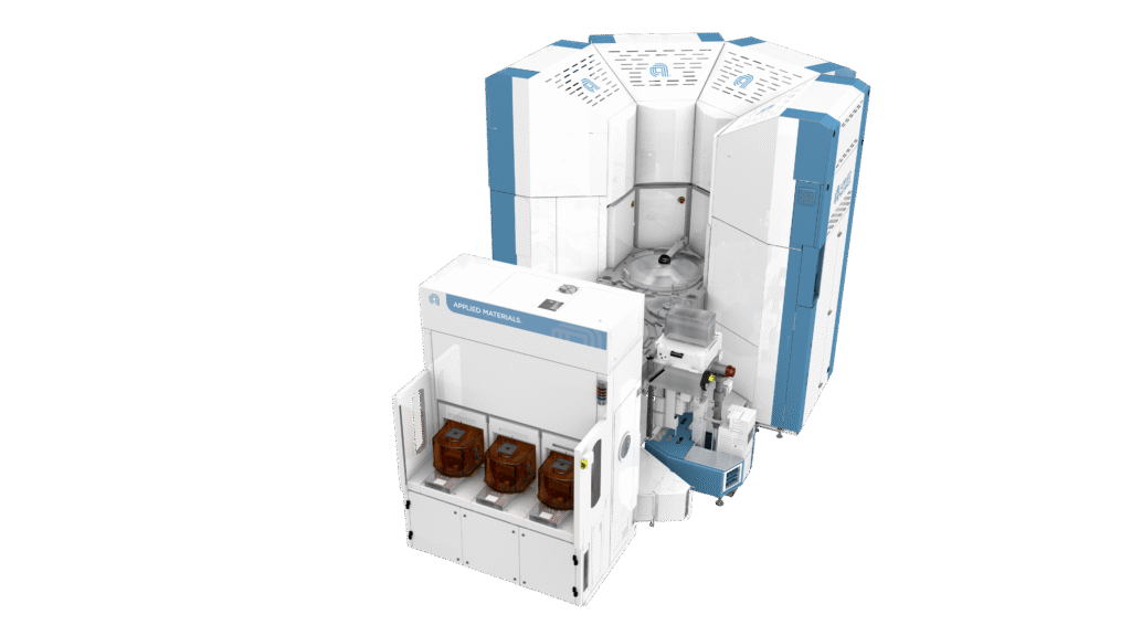
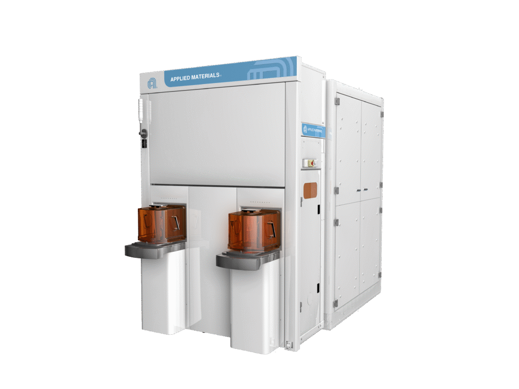
Kinex Bonding System
Recently, GPUs and high performance computing (HPC) chips utilize advanced packaging schemes to combine multiple chiplets into complex systems to optimize performance and power efficiency.
For that reason, hybrid bonding is an emerging chip-stacking technology because it uses direct copper-to-copper bonds. Therefore, yielding improved performance and reduced power usage at lower cost.
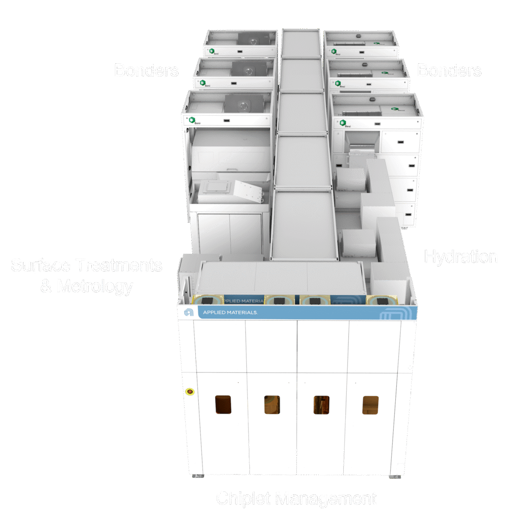
However, complex chip packages create challenges for hybrid bonding in high-volume manufacturing scenario. Because of this, Applied Materials, along with BE Semiconductor Industries N.V. (BESI), developed the Kinex Bonding system, the first integrated die-to-wafer hybrid bonder.
The Kinex system is currently being used by multiple logic, memory and OSAT customers.
Centura Xtera Epi System
The source and drain structures are among the critical features affecting the performance of GAA transistors. Specifically, the source and drain are created by precisely depositing materials in deep trenches using an epitaxial (epi) process. However, the process of filling the high aspect ratio source/drain trenches using conventional epi is challenging and can lead to voids and uneven growth, which reduce the performance and reliability of GAA transistors.
Consequently, Applied Materials’ latest Centura Xtera Epi system aims to address these challenges. The Xtera system features a unique low-volume chamber architecture which includes integrated pre-clean and etch processes to enable void-free GAA source-drain structures with 50 percent lower gas usage than conventional epi.
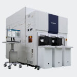
PROVision 10 eBeam Metrology System
Of late, there has been an increasing use of 3D architectures in logic and memory that create new metrology challenges and pushing optical technology to the limits. Hence, Keith Wells, Group Vice President of Imaging and Process Control at Applied Materials said the new PROVision 10 eBeam metrology system of the company is a purpose-built for advanced logic chips, including GAA transistor and Backside Power Delivery architectures as well as DRAM and 3D NAND chips.
It is the industry’s first metrology system to feature cold field emission (CFE) technology, which increases nanoscale image resolution by up to 50 percent and imaging speed by up to 10X compared to conventional thermal field emission (TFE) technology. The PROVision 10 system’s sub-nanometer imaging capabilities allow it to see through multiple layers of 3D chips and provide an integrative, multi-layer image.
“Applied is extending its eBeam leadership with breakthroughs in imaging resolution, deep into the 3D architecture at high throughput, giving chipmakers the ability to obtain precise measurements and accelerate yield of complex chip designs,” said Wells.
09 October 2025
- Share: