ASIA ELECTRONICS INDUSTRYYOUR WINDOW TO SMART MANUFACTURING
Applied Materials, Ushio Launch New Digital Lithography Tool for AI Era
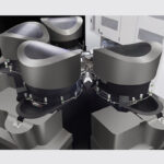
Applied Materials, Inc. and Ushio, Inc. jointly announced a strategic partnership to accelerate the industry’s roadmap for the heterogeneous integration (HI) of chiplets into 3D packages. The companies are jointly bringing to market the first digital lithography system specifically designed for patterning the advanced substrates needed in the artificial intelligence (AI) era of computing.
Rapidly growing AI workloads are driving the need for larger chips with greater functionality. In fact, the performance requirements of AI outpaces traditional Moore’s Law scaling. Amid this, chipmakers are increasingly adopting HI techniques, which combine multiple chiplets in an advanced package. Specifically, this aims to deliver similar or higher performance and bandwidth as a monolithic chip. The industry needs larger-package substrates based on new materials such as glass that enable extremely fine-pitch interconnects and superior electrical and mechanical properties. Thus, the strategic partnership between Applied and Ushio brings together two industry leaders to accelerate this transition.
“Applied’s new Digital Lithography Technology (DLT) is the first patterning system that directly addresses the needs of our customers’ advanced substrate roadmaps,” said Dr. Sundar Ramamurthy, Group Vice President and General Manager of HI, ICAPS and Epitaxy, Semiconductor Products Group at Applied Materials. “We are leveraging our unmatched expertise in large substrate processing, the industry’s broadest portfolio of HI technologies, and deep R&D resources to enable a new generation of innovation in high-performance computing.”
“Ushio brings over 20 years of experience building lithography systems for packaging applications, with more than four thousand tools delivered worldwide,” said William F. Mackenzie, Group Executive Officer and General Manager, Photonics Solutions Global Business Unit at Ushio. “With this new partnership, we can accelerate adoption of DLT through our scalable manufacturing ecosystem and robust field-service infrastructure, and broaden our portfolio to provide more solutions to the rapidly evolving challenges in packaging technology.”

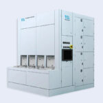
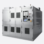
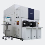
Mainly, the new DLT system is the only lithography technology that can achieve the resolution necessary for advanced substrate applications while delivering throughput levels required for high-volume production. It can pattern less than 2-micron line widths. Accordingly, the system enables the highest area density for chiplet architectures on any substrate. These include wafers or large panels made of glass or organic materials. Moreover, the DLT system is uniquely designed to solve unpredictable substrate warpage issues and achieve overlay accuracy.
The company has shipped production systems to multiple customers. Also, it has demonstrated 2-micron patterning on glass and other advanced package substrates.
Applied pioneered the technology behind the DLT system. The company will be responsible for R&D and the definition of a scalable roadmap together with Ushio to enable continued innovation in advanced packaging to 1-micron line widths and beyond. Meanwhile, Ushio will leverage its mature manufacturing and customer-facing infrastructure to accelerate the adoption of DLT. Together, the partnership offers customers the broadest portfolio of lithography solutions for advanced packaging applications.
- Share: