ASIA ELECTRONICS INDUSTRYYOUR WINDOW TO SMART MANUFACTURING
How Atomic Precision Is Changing Chip Manufacturing
As semiconductor devices approach atomic dimensions, the industry is confronting a transition unlike any before. The move from nanometer to angstrom‑scale manufacturing is not just another node shrink—it demands fundamentally new approaches to equipment design, process control, and development speed.
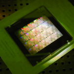
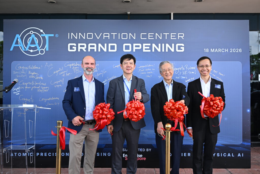
Deep tech startup Applied Angstrom Technology (AAT) has recently opened its Atomic Precision Innovation Center (APIC) in Singapore, a purpose-built facility focused on angstrom‑scale semiconductor manufacturing equipment. This enables AAT to mount complete etch systems for the angstrom era under one roof.
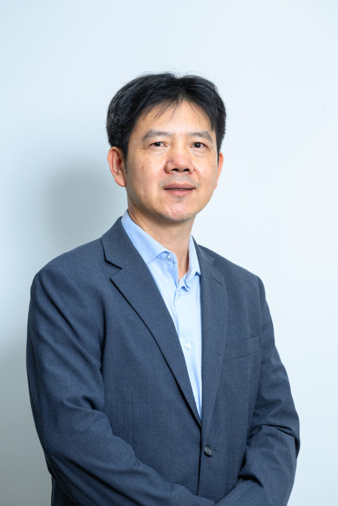
Dr. Richard Yang is the CEO of AAT, which he founded in 2022 to address the inflection point of the next‑generation semiconductor node. In this exclusive interview with AEI, Dr. Yang explains why atomic‑level precision is becoming non‑negotiable, how AI‑native equipment changes the economics of advanced fabs, and why agility matters in an industry dominated by giants.
“The chips that power AI require equipment that is itself powered by AI. Today, AI not only drives chip demand—it drives how semiconductor equipment is designed and built.” — Dr. Richard Yang, Founder and CEO, Applied Angstrom Technology
AEI: What defines AAT’s identity in the semiconductor equipment ecosystem—and why a specialized, agile player like AAT is essential in the angstrom era?
Dr. Yang: When I started AAT in 2022, that was the start of the transition from 3nm and 5nm FinFET to 3D gate‑all‑around transistors—nanosheets and nanoribbons. That is where angstrom precision becomes critical.
We started this equipment company as a clean‑sheet innovation. We did not rely on traditional tool architectures. We also built an AI‑native equipment platform. We were early pioneers in this space using agentic AI for process tuning, which is a very critical part of equipment performance.
Another part of our identity is how we accelerate equipment development using a physical AI stack. Those are our differentiators: clean‑sheet equipment design, AI‑native architecture, and acceleration through a physical AI stack.
AEI: How do you define the shift from the nanometer era to the angstrom era and why is atomic layer etching becoming a must‑have tool at 1.4 nm and beyond?
Dr. Yang: Etching started in the 1980s. At micron scale, it was bulk removal. Over the past decades, we entered the nanometer era, down to five and seven nanometers. Traditional etching could barely meet precision requirements at those nodes. At three nanometers, two nanometers, and beyond 1.5 nanometers, you have to count atoms. Precision at the atomic level becomes mandatory.
When I started working on this 10 years ago, we called it pseudo‑atomic layer etching—etching a few monolayers at a time. At seven nanometers, only one or two critical layers required that precision. Today, at three nanometers, more than ten steps already require atomic‑layer precision. Atomic-layer etching has become a must‑have technology for logic.
AEI: Does atomic‑level precision inherently sacrifice manufacturing speed—and how does AAT address throughput?
Dr. Yang: In traditional tools, there is a clear trade‑off between precision and speed. Throughput drops significantly. For the same application, moving from traditional etching to atomic‑layer etching can be five times slower.
That is why we started with a clean‑sheet design. We developed a new architecture specifically for atomic‑layer‑by‑atomic‑layer etching. With this approach, we can achieve the required precision and regain throughput. We can achieve the same etching results at ten times the speed.
AEI: How does atomic‑layer processing impact yield, given the risks of defects at angstrom‑scale dimensions?
Dr. Yang: We have to ensure very high repeatability. Each layer‑by‑layer step must behave consistently. Physically, we use self‑limiting reactions that only modify a single layer, and we precisely control energy to remove just one monolayer. That performance has been demonstrated through our hardware innovations.
On the software side, we rely on real‑time process control to ensure repeatability, along with sensing mechanisms that can detect and correct defects.
AEI: Does this make atomic‑layer etching viable for high‑volume giga fabs?
Dr. Yang: Yes. This is the direction our customers are interested in, and it is what we are driving toward. It will take time to mature—hardware reliability, uniformity, and other requirements—but this is clearly the path forward.
AEI: As transistors scale vertically, sidewall and edge uniformity become critical. What differentiates your approach?
Dr. Yang: Uniformity exists both laterally—across the wafer—and vertically, from top to bottom of the structure. We select self‑limiting chemistries that ensure consistent reactions from top to bottom. Another key differentiator is achieving a sufficiently high density of reactive species so they can transport effectively through high‑aspect‑ratio structures. That capability is built into our chamber design.
AEI: How does AI‑embedded hardware improve reliability of the etch system at angstrom level?
Dr. Yang: At the angstrom level, complexity increases significantly. Legacy tools struggle because complexity grows by orders of magnitude when moving to layer‑by‑layer processes.
We took a different approach by decoupling controls as much as possible, so each step performs a clearly defined function. This allows much more precise control and enables algorithm‑driven optimization. With this design, we can apply advanced control algorithms and begin using agentic AI approaches for process development.
AEI: Can these technical advantages help AAT compete against industry heavyweights?
Dr. Yang: Definitely. We designed AAT as a clean‑sheet, AI‑native company from the beginning. Traditional players are burdened by legacy architectures, similar to internal combustion engines versus electric vehicles. As a startup, we can innovate faster and move much more quickly.
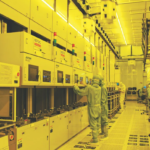
AEI: What is the strategic importance of your new R&D facility in Singapore?
Dr. Yang: Singapore already accounts for about 20 percent of global semiconductor equipment shipments. It has a mature manufacturing base, strong infrastructure, and both multinational and local semiconductor companies. The new APIC Center allows us to design, test, and demonstrate tools locally, which is why we received support from Enterprise Singapore. Advanced fabs are also moving cutting‑edge development to Singapore, including Micron’s advanced 3D NAND work.
This center enables close collaboration with customers, creating a fast feedback loop that improves our tools and strengthens the local ecosystem.
Asia is also where most fabs are located—Taiwan, Japan, Korea, China—so being in Singapore brings us much closer to end customers than the US or Europe.
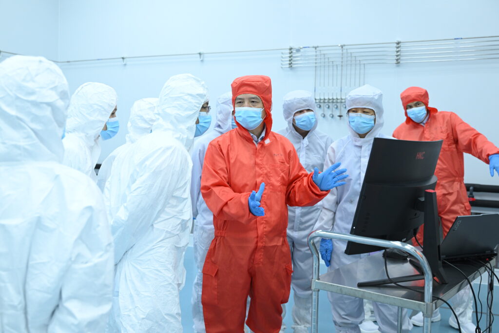
AEI: How does the facility support high‑risk pathfinding experiments for tier‑one foundries?
Dr. Yang: Development speed is critical. In a fab, each wafer is expensive—sometimes a single mask can cost over US$10,000. At our facility, we can cut wafers into hundreds of pieces and run many experiments at about 1 percent of the cost. This allows two orders of magnitude more experiments per wafer compared to a fab environment.
AEI: Will the transition from nanometer to angstrom be as smooth as earlier node transitions?
Dr. Yang: The transition from micrometer to nanometer was relatively smooth. Wafer size scaled from 200mm to 300mm, and many companies grew during that shift.
The nanometer‑to‑angstrom transition is much harder. Wafer size will not scale beyond 300mm. That is no longer economically viable. The progress depends entirely on atomic precision. Devices are also stacking in three dimensions, requiring precise control in X, Y, and Z directions. This transition is far more difficult; it is driven by physics and chemistry.
This transition will test hardware architecture, extensibility, and software control. That is why we entered the market with atomic etching as our first product and designed our systems to decouple process control while leveraging agentic and physical AI.
AEI: Is AI‑driven compute demand increasing pressure on equipment manufacturers and how does AAT try to meet this demand?
Dr. Yang: We are seeing supply chain pressure and longer lead times as demand strengthens. Another challenge is engineering new subsystems that can work seamlessly with next‑generation hardware.
We are developing physical AI stacks to simulate uniformity and optimize chamber design. During hardware reliability testing—what we call marathon or Ironman mode—AI plays a critical role in accelerating validation.
AEI: What does AAT’s product roadmap look like?
Dr. Yang: We follow a standard product lifecycle: prototype, alpha, beta, and production. We are entering markets in stages—starting with memory, then expanding into logic and adjacent sectors such as silicon photonics and quantum computing.
Atomic etching follows a familiar pattern: it begins as a niche technology and then expands into broader adoption. This year is very busy for us. Our product is moving beyond beta, and we are expanding from memory into another sector. Beyond next year, we expect wider adoption of atomic etching.
AAT’s position is unique. We are a clean‑sheet, AI‑native equipment company. The chips that power AI require equipment that is itself powered by AI. Today, AI not only drives chip demand—it drives how semiconductor equipment is designed and built.
07 April 2026
Cristian Canoza
- Share: