



ASIA ELECTRONICS INDUSTRYYOUR WINDOW TO SMART MANUFACTURING
Fujifilm Opens New AI Chip Materials Line in Oita
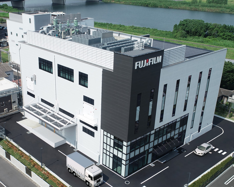
Fujifilm has completed and begun operations at a new production building dedicated to advanced semiconductor materials at its Oita manufacturing site in Japan, a move designed to significantly increase capacity for the fast-growing artificial intelligence semiconductor market.
The new facility, operated by Fujifilm Electronic Materials Co., Ltd. (FFEM), entered operation in August and focuses on the production of post-CMP cleaners, a critical semiconductor manufacturing material used after chemical mechanical polishing (CMP) processes.
Capacity Expansion Targets AI Semiconductor Growth
The investment reflects accelerating demand for advanced semiconductors driven by the expansion of AI, 5G and Internet of Things technologies. Fujifilm said the new building will substantially strengthen its ability to supply post-CMP cleaners used in leading-edge semiconductor manufacturing.
Post-CMP cleaners remove particles, trace metals and organic residues while protecting metal surfaces after polishing processes. As chipmakers continue to pursue greater miniaturization and multilayer device structures, demand for these materials is increasing alongside demand for CMP slurries, another key semiconductor consumable.
According to the company, the new facility incorporates automated manufacturing systems and quality evaluation equipment designed for the extremely high purity requirements of advanced semiconductor materials. The project will expand production capacity at the Oita site to three times previous levels.
Semiconductor Materials Business Continues Strong Momentum
Fujifilm identified semiconductor materials as one of its core growth businesses. The company reported that revenue from the segment grew at an average annual rate of approximately 20% between fiscal 2021 and fiscal 2025.
To support that growth, Fujifilm invested more than ¥100 billion in the business between fiscal 2021 and fiscal 2024. Recent initiatives have included expanding CMP slurry production capacity in Japan, the United States and Taiwan, as well as increasing polyimide manufacturing capacity in Japan and Belgium.
The company is continuing growth investments across Japan, North America, Europe and Asia during fiscal 2025 and 2026 as global semiconductor demand rises.
Strengthening Global Supply Capabilities
Fujifilm expects strong long-term growth for post-CMP cleaners, forecasting sales of the product category to more than double by fiscal 2030 compared with fiscal 2024 levels.
The company markets a broad portfolio of semiconductor process materials ranging from photoresists and photolithography-related chemicals to CMP slurries, post-CMP cleaners, thin-film materials, polyimide-based insulating materials and high-purity process chemicals. These products support semiconductor production from front-end wafer fabrication through advanced packaging processes.
In addition to expanding manufacturing capacity, the new Oita building features rooftop solar panels aimed at increasing the use of renewable energy and reducing greenhouse gas emissions associated with plant operations.
By combining expanded manufacturing capabilities, global production sites and research and development resources, Fujifilm aims to strengthen support for semiconductor manufacturers worldwide as demand for advanced chips continues to grow.
27 August 2026
- Share: