



ASIA ELECTRONICS INDUSTRYYOUR WINDOW TO SMART MANUFACTURING
Beyond Fabs: How SEMICON India Marked the Shift to a Complete Value Chain
SEMICON India 2026 concluded with major momentum, securing approximately $7B in investment commitments and outlining a path toward a $200B market by 2035. Driven by the ₹1.27,500 crore Semicon 2.0 framework, India is transitioning from individual fabs to a fully integrated ecosystem spanning materials, packaging, and design. Read our full post-show executive report.
SEMICON India 2026 closed its fifth and biggest edition yet at Yashobhoomi, New Delhi, yielded 54 strategic partnerships, alongside approximately US$7 billion in investment commitments, signaling a distinct shift in the region’s technological strategy.
This momentum aligns with the rollout of Semicon 2.0. Backed by an outlay of ₹1,27,500 crore ($15.2 billion), the state initiative addresses six core pillars: design, equipment and materials, fabrication facilities, advanced packaging, R&D, and talent.
The event was organized by global industry organization SEMI and the India Semiconductor Mission (ISM) with India Electronics and Semiconductor Association (IESA) as a strategic partner.
“The semiconductor story in India has moved from ambition to action, from announcements to commercial production—and from individual projects to an ecosystem,” said Ashok Chandak, President of SEMI India and IESA. “Semicon 2.0 gives us the policy runway. SEMICON India gives the industry a platform to connect, invest, partner and execute.”
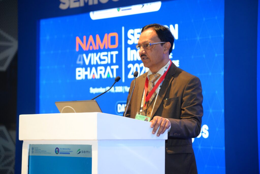
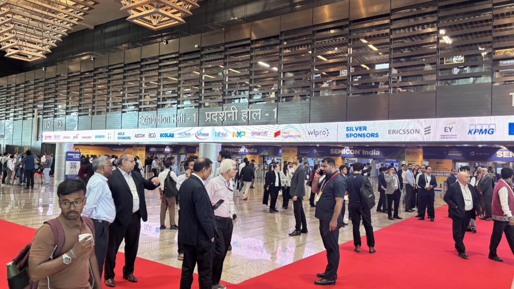
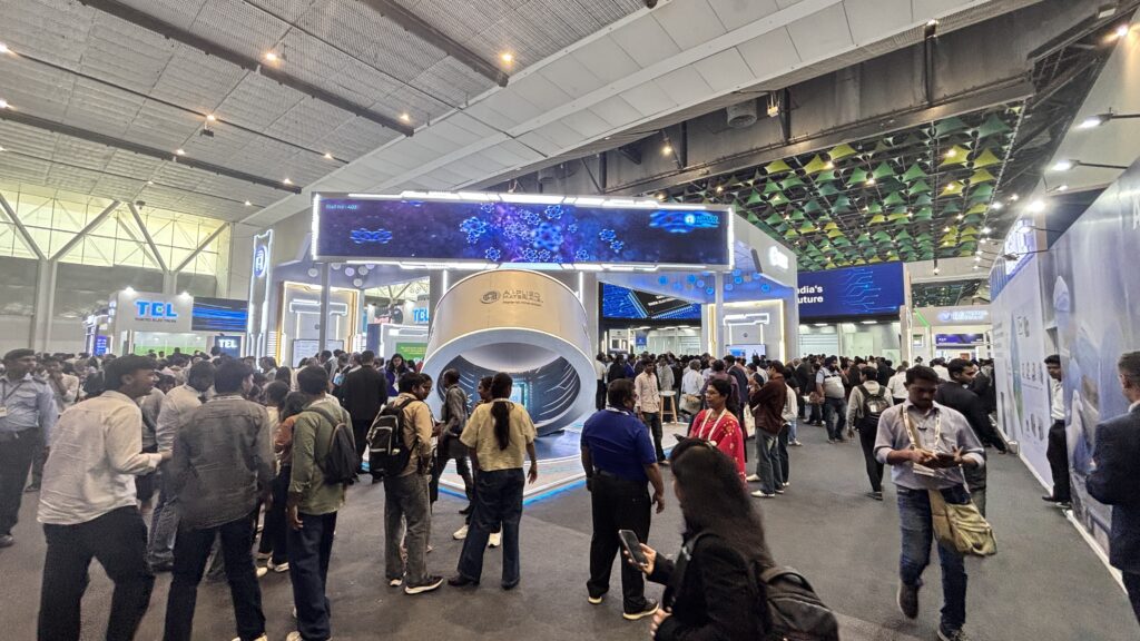
Over three days, the conference drew 51,656 registrations, approximately 40,000 cumulative visitors, and more than 600 exhibitors. Around 300 international companies across 52 participating nations engaged in over 5,000 B2B discussions.
The Market Realignment
During the SEMICON India 2026 week, IESA and Ernst & Young (EY) India released a joint report titled Semicon India 2.0: From Capacity Creation to Ecosystem Leadership, which projected India’s domestic chip market to expand threefold, rising from nearly US$64 billion in 2026 to US$200 billion by 2035. The 2035 projection essentially doubles an earlier projection made by IESA that the industry will hit US$100 billion by 2030.
The report also said consumer electronics accounts for 30 percent of Indian semiconductor demand in 2025, with automotive and industrial sectors consuming 16 percent and 15 percent, respectively. Rapid growth in artificial intelligence, data centers, telecommunications, and electric mobility is accelerating this trajectory.
Between FY17 and FY25, semiconductor imports grew at a 23 percent CAGR, rising from US$5.7 billion to US$30.3 billion. Capturing this expanding demand requires converting design strengths into localized hardware. India currently contributes nearly 20 percent of the global chip design engineering workforce, offering an established engineering base to support manufacturing scale-up.
“India has a powerful combination of market scale, engineering talent and policy momentum,” noted Aisha Ali Hussaini, Partner and Semiconductor Tax Leader at EY India. “The priority now is to translate this scale into deeper semiconductor value addition by building a connected, innovation-led ecosystem that attracts sustained investment and creates more value domestically.”
Before you move on, you might also like:
How we covered SEMICON India 2026:
SEMICON India 2026 Powers New Era of Chip Collaboration
Semicon 2.0 Powers India’s Chip Ecosystem Expansion
SEMICON India 2026: Chip Investors Rally Behind India’s Next Growth
Curtains Close as SEMICON India Charts Bold Chip Growth
Localizing Supply Chains
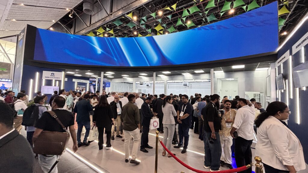
A key focus of SEMICON India 2026 was domestic supply chain integration. For one, Tata Electronics announced strategic agreements across the value chain, including partnerships covering wafer manufacturing, assembly and testing, advanced packaging, photoresists, and high-purity gases. To centralize supplier infrastructure, Tata Electronics partnered with Ascendas First Space to establish a 363-acre Vendor Park in Dholera, Gujarat.
Local material sourcing gained traction through collaborations targeting specialized inputs. Tata Electronics signed MoUs with Inox Air Products for high-purity gases, Sumitomo Chemical for specialized process chemicals, Fujifilm Corporation for materials, and Enomoto Co. for lead-frame manufacturing. C-MET and Hindalco Industries announced a joint effort to develop critical raw materials locally.
Equipment and infrastructure engineering were addressed through partnerships with Kelington Engineering for gas distribution systems and Besi Singapore for advanced packaging technologies. Additional agreements involved OSAT/ATMP providers securing long-term capacity bookings, while fabless firms like L&T Semiconductor Technologies showcased localized Silicon Carbide power modules and smart metering solutions.
Commercial Fabs and R&D Execution
The transition to physical production advanced with the inauguration of commercial packaging lines at CDIL Semiconductor in Mohali and Suchi Semicon in Surat. These facilities bring the count of operational commercial units under the original Semicon program to five. The government estimates that current Semicon 2.0 operations and investment indications will generate nearly 100,000 direct and indirect jobs.
Deep-tech funding saw expanding commitments. The India Deep Tech Alliance announced US$236 million in direct investments spread across 56 deep-tech firms. On the design side, the launch of six ChipIN Regional Centres aims to broaden access to open-source PDKs and EDA tools for regional innovators. C-DAC launched the SC-VEGA-SOM, an indigenous System-on-Module combining C-DAC’s VEGA processor with IndieSemiC’s LoRa RF module.
Our Exclusive Interviews at SEMICON India 2026
Silicon to Systems: India’s US$200B Chip Blueprint
SEMI: India to Rise as Global Chip Powerhouse
Delta Scales Up Smart Tech for India’s Chip Push
Resonac Eyes India’s Future Packaging Potential
Advantest Scales Up Test Solutions for India’s Chip Market
ASMPT Powers India Across Full Packaging Spectrum
Emergence of 200 Chip Design Companies
During a press conference, Ashwini Vaishnaw, India’s Union Minister for Electronics and Information Technology, outlined the next phase of the country’s semiconductor strategy.
“India’s semiconductor mission has moved from proving intent to execution at scale,” he said.
Design remains a major pillar of India’s semiconductor ambitions. The minister projected the emergence of at least 200 chip design companies under ISM 2.0 and described the sector as a “game changer” for creating indigenous semiconductor intellectual property. More than 105 design startups have already gained access to advanced Electronic Design Automation tools, while 20 startups have secured venture funding. Around 70,000 chip-design engineers have also been trained over the past four years.
According to the minister, ISM 2.0 will build on the foundation established under the first phase of the India Semiconductor Mission through six focus areas: design, machines and materials, new fabrication facilities, strengthening the ATMP/OSAT industry, research and development, and talent development. He noted that ISM 1.0 achieved its objectives in four years despite being originally planned as a six-year program, and expressed confidence that the next phase would advance at a similarly accelerated pace.
— Cristian Canoza
28 September 2026
- Share: