



ASIA ELECTRONICS INDUSTRYYOUR WINDOW TO SMART MANUFACTURING
U.S.-Japan Initiative Expands GF Manufacturing
GlobalFoundries is set to play a broader role in U.S. semiconductor expansion efforts after being selected as the technology provider and operator for two planned semiconductor fabrication facilities in New York under a U.S.-Japan initiative that could provide up to $21 billion in funding.
The announcement adds significant new manufacturing capacity to the company’s New York operations while also bringing together Japanese investment, U.S. government support, and foundry manufacturing expertise under a single framework. The project is intended to strengthen domestic semiconductor production and support supply chains serving automotive, industrial, and connected infrastructure markets.
Capacity Expansion Moves Forward
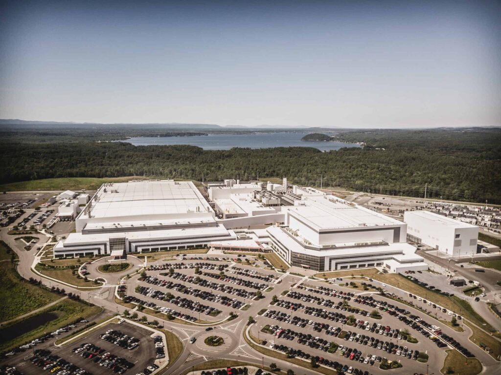
An initial investment of approximately $10 billion is expected to accelerate construction of a new 300mm fab at GF’s Malta, New York campus, with operations targeted for 2029. A second investment of roughly $10 billion could fund another fab at the site. Together, the facilities would substantially increase U.S. semiconductor manufacturing capacity.
When fully operational, the first fab is expected to add approximately 900,000 300mm wafers of annual capacity. A second fab would add a similar amount. The project is also expected to generate about 27,000 construction and ecosystem jobs as well as more than 1,000 manufacturing jobs in New York’s Capital Region.
“This is a bold new initiative for semiconductor manufacturing, bringing together the United States and Japan with GF’s differentiated technology and decades of manufacturing expertise to accelerate trusted capacity in New York,” said Tim Breen, CEO of GlobalFoundries. “GF was selected because fabs of this scale require more than capital. They require differentiated technology, operational excellence and a proven ability to execute.”
Investment Extends Beyond Wafer Production
Alongside the new fab plans, GF said it has reached an agreement with the U.S. Department of Commerce to amend its existing CHIPS and Science Act award, reallocating $955 million to accelerate investments in silicon photonics, silicon-germanium and advanced packaging at facilities in New York and Vermont. The company said these technologies are becoming increasingly important for communications infrastructure and data-center applications.
The announcement therefore combines capacity expansion with additional investment in specialized manufacturing capabilities that support emerging semiconductor applications.
Customers and Partners Back Expansion
Several industry partners emphasized the strategic importance of expanding U.S.-based manufacturing capacity.
“We are planning around GF’s new capacity in New York as an extension of Renesas’ own production footprint,” said Hidetoshi Shibata, CEO of Renesas. “This expanded collaboration further strengthens the stable, long-term supply of semiconductors.”
Tony Kawai, president and CEO of Tokyo Electron, noted that resilient semiconductor manufacturing depends on a trusted ecosystem of equipment and technology partners and described the project as reflecting the close collaboration between the United States and Japan within the global semiconductor industry.
GF expects to break ground on the first fab later this year at its Malta site, which the company said is already permitted and equipped with existing infrastructure.
15 October 2026
- Share: