
ASIA ELECTRONICS INDUSTRYYOUR WINDOW TO SMART MANUFACTURING
UVJC Targets Manufacturing Shift With NovaJet
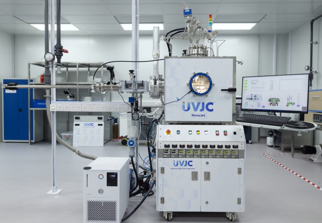
Singapore-headquartered Universal Vapor Jet Corporation’s (UVJC) launch of NovaJet marks more than the introduction of another semiconductor manufacturing tool. It represents the first commercial deployment of its proprietary Universal Vapor Jet Printing (UVJP) technology and a significant step in moving the platform from research environments into real-world manufacturing applications.
Developed and built in Singapore, NovaJet is the first commercial system based on UVJC’s UVJP platform. The company, a wholly-owned subsidiary of U.S.-headquartered Universal Display Corporation (UDC), positions the technology as a dry, solvent-free and maskless deposition approach that allows researchers, process engineers and manufacturers to evaluate advanced materials, develop deposition processes and validate applications before progressing toward larger-scale production.

UVJC sees NovaJet as a complementary tool that could help bridge one of the persistent challenges in semiconductor and advanced manufacturing industries: the gap between materials discovery and manufacturing deployment. The company’s longer-term vision includes supporting customers as validated processes move from laboratory environments into customized production-scale UVJP systems.
“As industries pursue increasingly advanced materials and device architectures, bridging the gap between innovation and manufacturing has become essential,” said Chandran Nair, Chief Executive Officer of UVJC. “NovaJet was designed to give researchers, engineers and manufacturers a highly flexible platform for advancing new materials, developing processes and accelerating the path toward commercial production.”
In the following interview with AEI, Nair discusses the lessons learned during early validation work, UVJC’s manufacturing strategy, the role of NovaJet alongside conventional lithography, emerging opportunities in life sciences and clean-energy applications, and how AI could eventually help accelerate materials and process development.
AEI: What performance data or feedback from early lab implementations shaped the final production-ready system?
Nair: Our early validation work involved depositing coatings and printed patterns on a wide range of substrates, across several application areas. Four lessons shaped the production system.
The first was repeatability. Customers need to reproduce the same film consistently from run to run, so we placed strong emphasis on process control and thickness uniformity. The second was material flexibility. Researchers want to move between materials quickly, and to combine materials in a single run, without lengthy changeovers.
The third was temperature control, as substrates such as polymers, flexible materials, and biologically relevant surfaces are sensitive to high heat. NovaJet can operate without active substrate heating. Finally, ease of use was essential. The system is recipe-driven, allowing a team to reliably reproduce a process developed by another.
AEI: How is UVJC scaling manufacturing to support international orders without supply chain bottlenecks?
Nair: Design, assembly, integration and qualification are all carried out at our facility in Singapore. That gives us close control over quality and creates a short feedback loop between engineering and customers.
Our supply chain draws on well-established precision engineering suppliers and subsystems within the region’s strong semiconductor equipment ecosystem. The critical components that carry our core IP, notably the vapor jet print head, stay under our own control.
Our customer engagement model also helps us plan production and mitigate supply chain risks. Customers can begin developing and validating their process with us at our Singapore laboratory before taking delivery of their own tool.
“NovaJet is designed to complement, not replace, lithography. NovaJet brings a different set of capabilities, enabling precise deposition of functional materials where they are needed, without masks, solvents or high temperatures.”
— Chandran Nair, Chief Executive Officer of UVJC
AEI: How does NovaJet fit into existing semiconductor manufacturing workflows?
Nair: NovaJet is designed to complement, not replace, lithography. NovaJet brings a different set of capabilities, enabling precise deposition of functional materials where they are needed, without masks, solvents or high temperatures.
Because it is fully dry and solvent-free, it avoids wet chemistry, solvent handling and post-deposition bake within the deposition process. The process is also additive and maskless, so a pattern can be changed digitally through software without new tooling.
This makes NovaJet a complementary step for applications that can be challenging for conventional approaches, including depositing functional films on non-flat or three-dimensional surfaces, localized deposition in heterogeneous integration, and high-mix or low-volume applications where mask costs can be difficult to justify.
AEI: Which non-semiconductor vertical is showing the fastest traction, and how are you tailoring the platform to its regulatory or throughput demands?
Nair: Life sciences and biomedical applications are currently moving the fastest, particularly surface functionalization of medical devices and life science consumables.
The solvent-free process means solvent residues are not introduced during deposition, which is a meaningful advantage on materials destined for biological environments. We can also coat delicate and complex three-dimensional parts at low temperature.
Besides life sciences and biomedical applications, perovskite applications in clean-energy photovoltaics are a strategically important area for us, with active research engagements underway.
AEI: What AI-driven diagnostic or optimization modules are active in this commercial release?
Nair: NovaJet is built on a fully digital, recipe-driven control architecture that captures structured process data from every run. That provides an important foundation for these future AI-assisted capabilities.
Our focus is on using AI to accelerate materials and process discovery. Developing a new functional thin film can require many iterations of experimentation. By combining NovaJet process data with characterisation data and modeling of the vapor jet process, we aim to shorten the path from a candidate material to a validated, reproducible film.
AI-assisted process optimization remains under active development, with capabilities planned for progressive introduction to customers as development advances.
Cristian Canoza
09 November 2026
- Share: