ASIA ELECTRONICS INDUSTRYYOUR WINDOW TO SMART MANUFACTURING
Intel Marks Opening of US$3 Billion Factory Expansion
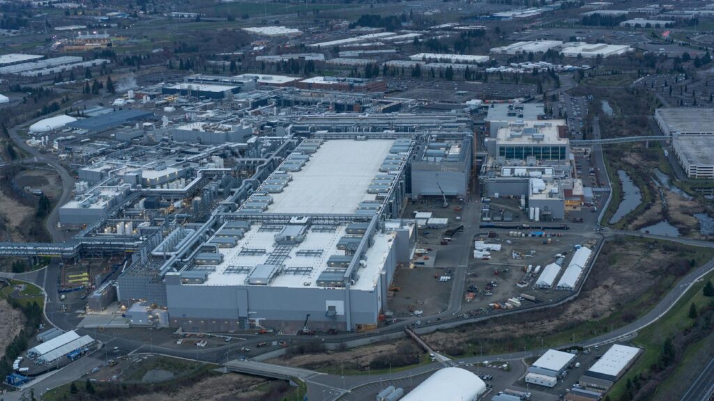
Intel Corporation has opened the latest expansion of D1X, its leading-edge factory in Hillsboro, Oregon. In addition, the company announced the new 500-acre campus will have a new name – Gordon Moore Park at Ronler Acres.
Gordon Moore Park is the headquarters of Intel’s global Technology Development organization, a team of about 10,000 employees responsible for advancing Moore’s Law by creating new transistor architectures, wafer processes, and packaging technologies.
To illustrate, the new name recognizes the site’s contributions to driving Moore’s Law, Intel co-founder Gordon Moore’s 1965 prediction that has guided innovation in the semiconductor industry for more than 50 years.
Bolsters IC Process Roadmap
In a ribbon-cutting ceremony attended by senior government officials and community leaders, Intel CEO Pat Gelsinger highlighted the company’s positive impact in Oregon and reiterated its commitment in semiconductor research and development (R&D). During the campus’s 25-year history, engineers and scientists have continually faced and overcame the challenges posed by physics when the features on a chip shrink to the size of atoms. With inventions like high-k metal gate technology, tri-gate 3D transistors and strained silicon, Intel has consistently delivered foundational process innovations to maintain pace with Moore’s Law.
“Since its founding, Intel has been devoted to relentlessly advancing Moore’s Law. This new factory space will bolster our ability to deliver the accelerated process roadmap required to support our bold IDM 2.0 strategy. Oregon is the longtime heart of our global semiconductor R&D, and I can think of no better way to honor Gordon Moore’s legacy than by bestowing his name on this campus, which, like him, has had such a tremendous role in advancing our industry,” said Gelsinger.
Last year, Intel unveiled one of the most detailed process technology roadmaps in itshistory. The company has moved to an accelerated pace of innovation to enable an annual cadence of improvements, leveraging breakthrough technologies that will power new products through 2025 and beyond, including RibbonFET, the first new transistor architecture in more than a decade; PowerVia, an industry-first new backside power delivery method; and the industry’s first use of High NA EUV next generation lithography.

Fosters Innovations
With “Mod3” – a more than US$3 billion investment to expand D1X – Intel engineers now have an additional 270,000 square feet of clean room space to develop next-generation silicon process technologies. At any given time, multiple logic process technologies are in various stages of the development cycle in the D1X factory. The Technology Development team creates the baseline manufacturing technology required to bring innovations into the physical world. New process technologies are then transferred identically from this central development factory in Oregon to Intel’s global network of high-volume manufacturing sites. After transfer, the network of factories and the development factory collaborate to continue driving operational improvements. This enables fast ramp of the operation, fast learning and better quality control.
This latest expansion builds on Intel’s nearly 50-year history of investing in Oregon. Intel’s operations in Oregon are its largest concentration of facilities and talent in the world, with close to 22,000 employees across four campuses in Hillsboro – 20 miles west of Portland. The Mod3 expansion brings Intel’s total investment in Oregon to more thanUS$52 billion.
- Share: