ASIA ELECTRONICS INDUSTRYYOUR WINDOW TO SMART MANUFACTURING
Lasertec Elevates Inspection of Under-Layer, Wafer Defects
Leveraging a broad range of inspection systems that support semiconductor manufacturing as mainstay products, Lasertec Corporation supports technological innovations in leading-edge fields. The company’s lineup of products supports the production of cutting-edge logic, memory, and compound power semiconductors. The company also puts forth its high technological expertise.
Lasertec recently announced two new inspection systems. Both systems enable inspection and review to detect defects in wafers with high accuracy. The company has developed these systems taking into consideration challenges in the latest semiconductor manufacturing processes. These systems contribute to improved quality and enhanced yields, meeting the needs of device manufacturers in the leading-edge semiconductor processes.
Defect Inspection Inside Devices
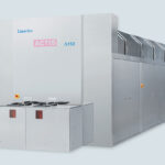
The CIRIUS Series High Sensitivity Under-layer Defect Inspection and Review System enables the inspection and review of defects that occur inside devices, a challenge that has emerged in the production of memory devices where higher integration is advancing. Through the adoption of the company’s proprietary optical technologies, the CIRIUS Series can inspect under-layer defects, capture their depth information and classify them based on it. These features enable non-destructive inspection and review of under-layer defects in devices. Thus, it contributes to the early-stage improvement of processes and the reduction of production costs.
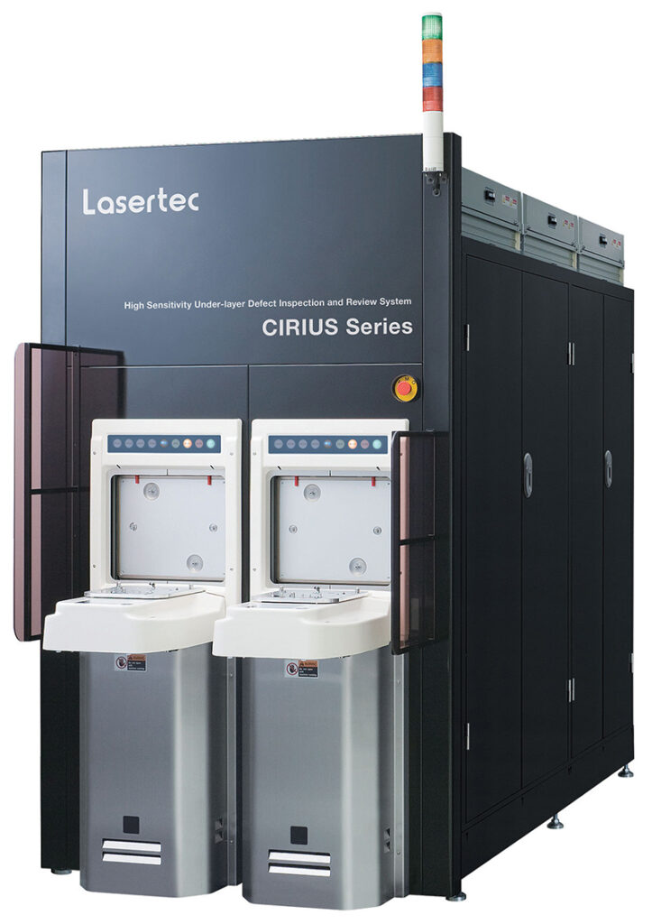
In the semiconductor manufacturing process, the effort to increase the number of layers in devices, such as three-dimensional (3D) NAND, has been advancing in parallel with the adoption of finer line widths. As a result, resolving the problem of defects inside devices (under-layer defects) has become a major challenge. The CIRIUS Series enables non-destructive inspection and review of under-layer defects, which was not possible with conventional inspection methods.
Stacking technologies have played key roles in devices with many stacked layers, such as 3D NAND flash memory. Moreover, they will also likely become important in the next-generation architecture of logic devices, such as gate all around (GAA), the development of which is currently under way.
Lasertec accelerates its effort to promote its systems around the world, aiming for their adoption in the manufacturing processes of state-of-the-art logic devices as well as in the processes of 3D NAND and other memory devices.
Identifies Defects at Wafer Edge
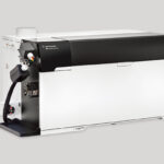
The CIEL Series High Sensitivity Wafer Edge Inspection System classifies defects at wafer edge and bevel with high accuracy. As the number of stacks in NAND memories increases and the design of logic devices becomes more complex, types of under-layer defects occurring due to defects at wafer edge have become diversified. Thus, a system that detects and identifies yield-critical defects among these diverse defects has been sought.
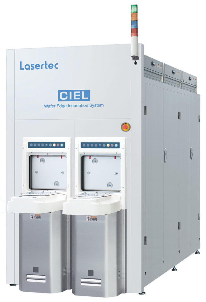
Lasertec has developed the CIEL Series by replacing the optics of the EZ300 system with newly developed ones to capture high-resolution color images for accurate defect identification and to achieve higher sensitivity and higher throughput. The CIEL Series uses deep learning technology for highly accurate defect classification and the 3D profiling function of the proprietary optics for capturing high-resolution images that include height and depth information, thereby enabling accurate detection and identification of defects of interest.
The CIEL Series identifies yield-critical minute defects that could not be detected and classified by conventional systems, helping customers improve semiconductor manufacturing processes.
Lasertec intends to continue meeting the needs of advanced semiconductor processes and contribute to improved quality and enhanced yield in the semiconductor manufacturing processes.
- Share: