ASIA ELECTRONICS INDUSTRYYOUR WINDOW TO SMART MANUFACTURING
Rigaku Harnesses X-Ray Tools for Advanced IC Process
Rigaku Corporation has been providing innovative X-ray products since its foundation in 1951 by utilizing its vertically integrated core technologies. Today, the company manufactures and ships more than 1,000 X-ray instruments annually. It continuously develops cutting-edge core technologies, such as rotating anode high-flux X-ray sources, multi-layer mirror optics, and 2D detectors in support of the company’s semiconductor technology development and high-volume manufacturing customers.
The world’s most advanced memory and foundry companies are present in Asia. As advanced devices reach nano-scale dimensions, along with higher density and three-dimensional architectures, Rigaku is working closely with its customers and further advancing the company’s technologies in order to meet their needs.
X-ray Metrology Tools
The following is Rigaku’s lineup of full wafer in-line metrology techniques. The company currently has an overall X-ray metrology tool global market share of more than 50 percent.
Among the metrology tools include X-ray Fluorescence (XRF) for film thickness and composition; Total X-ray Reflection Fluorescence (TXRF) for surface contamination; X-ray Reflectivity (XRR) for film thickness, density, and roughness; X-ray Diffraction (XRD) for crystallinity, stress, composition, and thickness; and Critical Dimension Small Angle X-ray Scattering (CD-SAXS) for CD metrology.
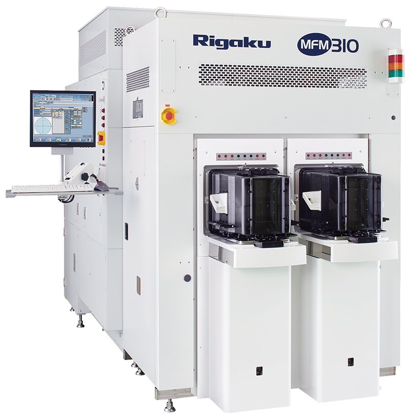
MFM310 Tool Series (Fig. 1)
The MFM310 tool series is a hybrid metrology system with micro-spot X-rays and a pattern recognition system, which is widely used in memory and logic fabs around the world. It has the capability of energy dispersive (ED) XRF, XRR and XRD measurements, and has enabled multipurpose metrology of thickness, composition, density, roughness, and crystallinity of various thin films.
Micro spot XRF
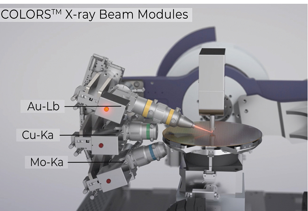
Its unique feature is the capability of three COLORSTM beam modules equipped on a goniometer (Fig. 2).
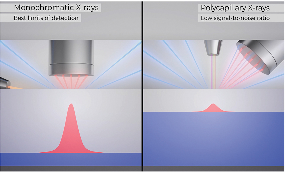
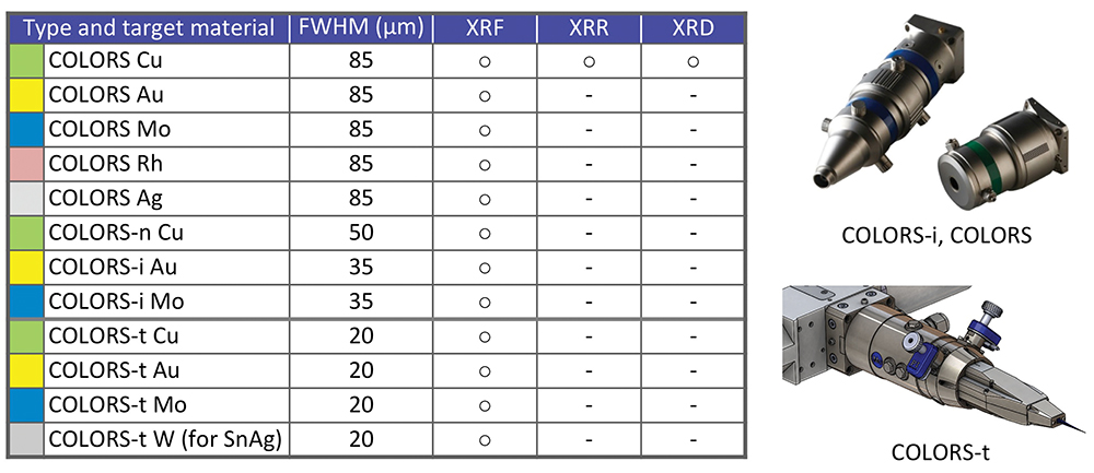
COLORSTM is a micro-focus X-ray module with multi-layer focusing mirror optics. Its monochromatic beam drastically reduces the Laue diffraction from silicon (Si) substrates and enables high signal-to-noise (S/N) XRF measurements for sub-nanometer thickness films (Fig. 3). COLORSTM has a variety of options in anode materials and beam spot diameters, so optimal configurations can be selected (Fig. 4).
COLORS-t with a 20µm FWHM beam size has been introduced to enable patterned active and test structure measurements for logic customers.
High-speed and high-precision XRR
A combination of a convergent X-ray beam by COLORS-Cu and utilization of Time Delay Integration (TDI) mode by Rigaku’s HyPix two-dimensional detector delivers a high precision and high throughput XRR measurement.
Onyx-3000 Tool Series
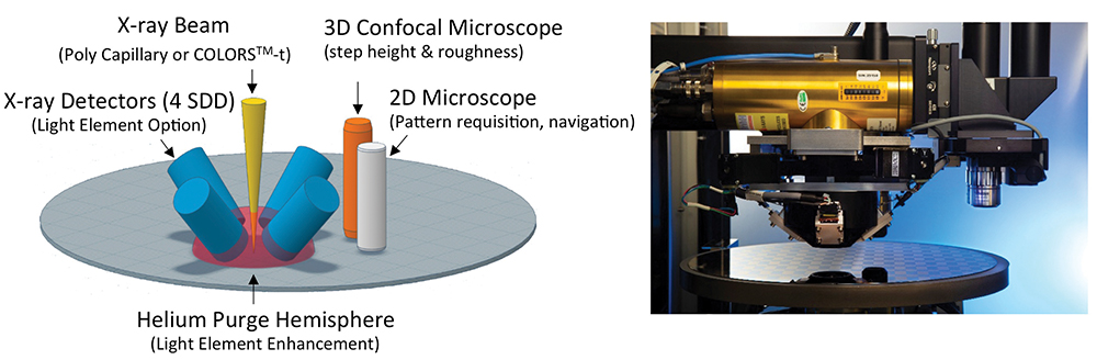
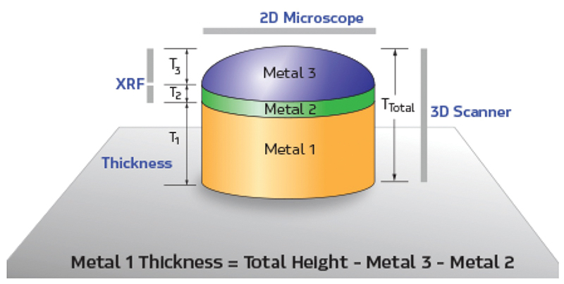
The Onyx 3000 tool is a new hybrid metrology capability developed by Rigaku and XwinSys. XwinSys was acquired by Rigaku in 2019 aimed at metrology solutions for ultra-fine patterned structures in front end of line (FEOL), back end of line (BEOL) and packaging processes. This tool can measure film thickness and composition of ultrathin films, patterned array structures and individual bumps by using micro spot ED-XRF. Larger structures with a few tens of micron height can be measured by an integrated 3D microscope (Fig. 4).
Micro spot ED-XRF
This tool can accommodate a polychromatic X-ray beam with a minimum spot size of 10µm delivered by polycapillary optics and also a 20µm monochromatic beam delivered by the previously described COLORS-t beam module. Furthermore, an X-ray beam module dedicated to tin-silver (SnAg) solder measurements is also available (Fig. 5). Smaller spot sizes less than 10µm are in development and will be equipped in the near future.
Helium purge function
A helium (He) purge sphere decreases the effect of absorption by air and enables XRF measurement of light elements like aluminum (Fig. 6).
3D microscope
The three-dimensional shape of micro-scaled features, such as solder bumps and copper (Cu) pillars can be measured using the incorporated 3D microscope. Also, hybrid measurements with ED-XRF enables thickness and composition of each layer of these micro-sized features with high accuracy and precision (Fig. 7).
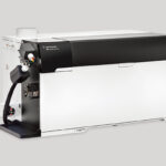
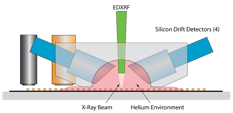
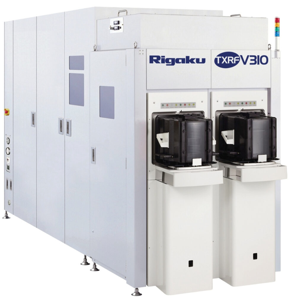
TXRF Tool Series (Fig. 8)
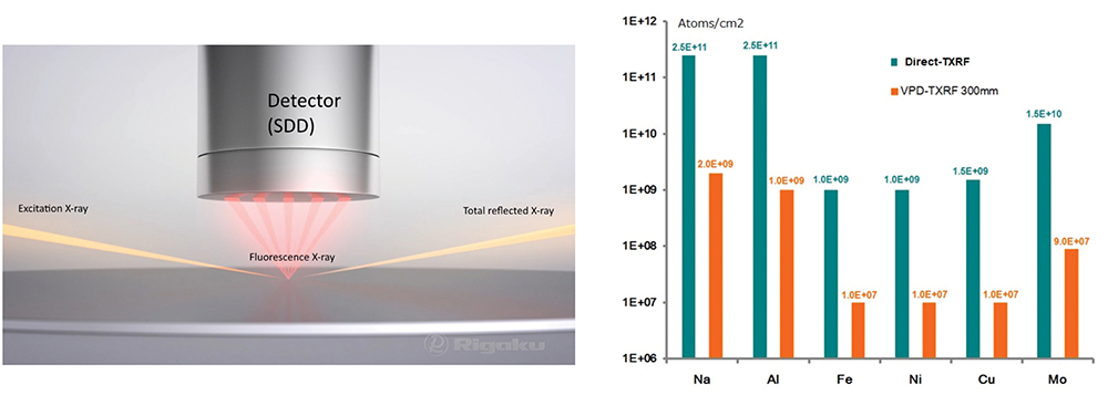
The TXRF tool series is an instrument line that analyzes wafer surface contamination with high sensitivity (PPM and PPB ranges). It is compatible with 100 to 300mm wafers and can analyze light elements (Na) to heavy elements (U) with high sensitivity. With TXRF, a superior S/N ratio can be obtained by utilizing monochromatic excitation X-rays at an angle lower than the critical angle at which a total reflection phenomenon occurs. As a result, a detection limit of 109 to 1010 atoms/cm2 level is achieved for most of the elements in the periodic table (Fig. 9).
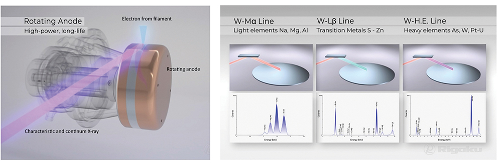
Advanced semiconductor processes, where new materials are being introduced, now require analytical capabilities spanning the range of light to heavy elements. The Rigaku TXRF tool series utilizes a high-power (9kW) rotating X-ray generator and high-reflectance monochromator (Fig. 10), which are a result of the company’s in-house core technology development efforts, and deliver the following features:
High sensitivity
The direct TXRF measurement method achieves a sensitivity level of 109 atoms/cm2 for transition metals (Fig. 9).
Wide-range elemental analysis
Three types of monochromators are automatically accessed according to the element of interest, and measurement is then performed with the optimal excited X-ray source (Fig. 10).
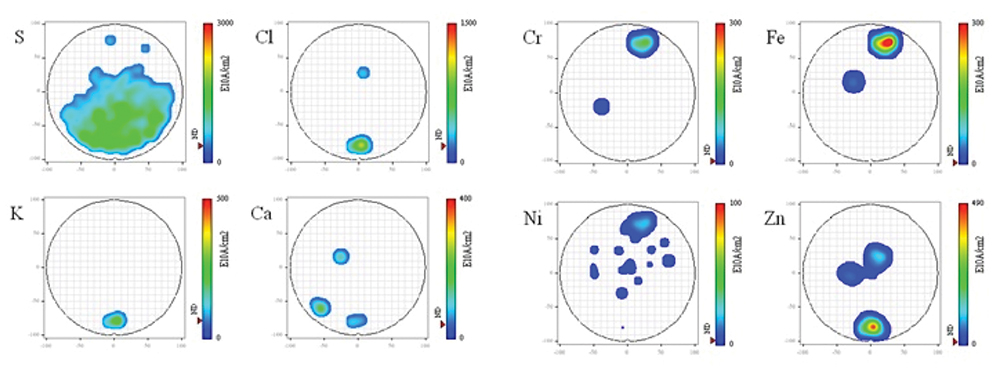
Fast scan mapping function (SWEEPING-TXRF)
With the bright source and optimized optics, only 30 to 40 minutes is required to map the entire surface of a 300mm wafer. Furthermore, the incident angle setting
error, which is caused by the motion of the sample stage, is corrected by a mathematical formula to maintain the high-speed and high-precision mapping (Fig. 11).
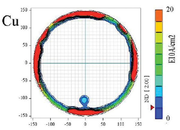
0mm edge exclusion function (ZEE-TXRF)
It is now possible to measure near the wafer edge where contamination is likely to occur (Fig. 12).
Wafer back-side measurement function (BAC-TXRF)
A wafer-reversing robot can be installed in the EFEM to enable automatic backside measurement of 300mm wafers.
Correlate TXRF contamination measurements with in-line wafer defect maps
It is now possible to import the coordinate data of defect inspection tools into the TXRF software platform and perform elemental analysis at the locations of the particles/defects (compatible with most defect inspection tools).
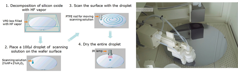
VPD-TXRF
By incorporating a vapor-phase decomposition (VPD) chemical pretreatment unit in the 300mm TXRF, ultra-high sensitivity analysis at the 107 atoms/cm2 level becomes possible (Fig. 13).
- Share: