ASIA ELECTRONICS INDUSTRYYOUR WINDOW TO SMART MANUFACTURING
Electronic Products Evolve as Manufacturing Advances
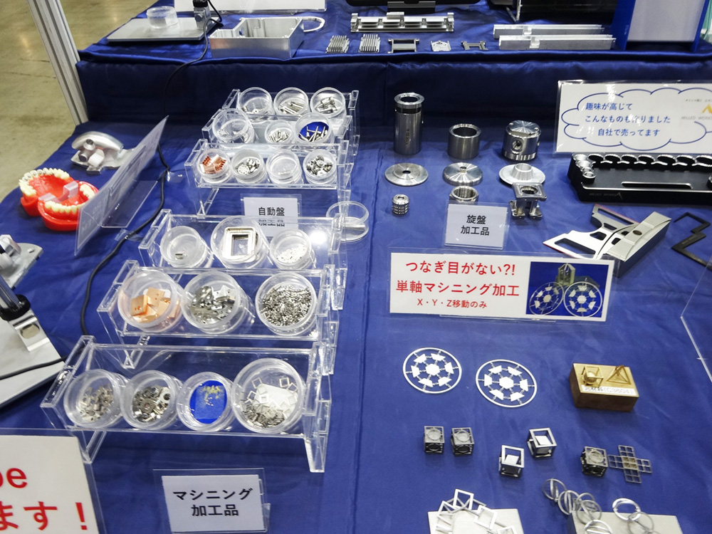
New electronic products arise from advancement of electric vehicles (EVs), internet of things (IoT) and digital transformation. Moreover, manufacturing technologies and processes continue to progress. Also, more industry newcomers tout their processing methods as new businesses are emerging.
Blue Laser Technologies in EVs
Blue laser light sources with high optical absorption efficiency are required for copper processing of motors and batteries. Conventional laser processing mainly uses laser light in the near infrared region. They include CO2 laser with wavelength of 10,600nm and YAG laser and fiber laser with 1,064nm. Meanwhile, blue lasers use wavelengths of 360 to 480nm in the ultraviolet region.
Blue lasers exhibit higher absorption rate for copper compared with infrared lasers. Specifically, they suit laser processing of copper materials commonly used for motors and batteries of EVs.
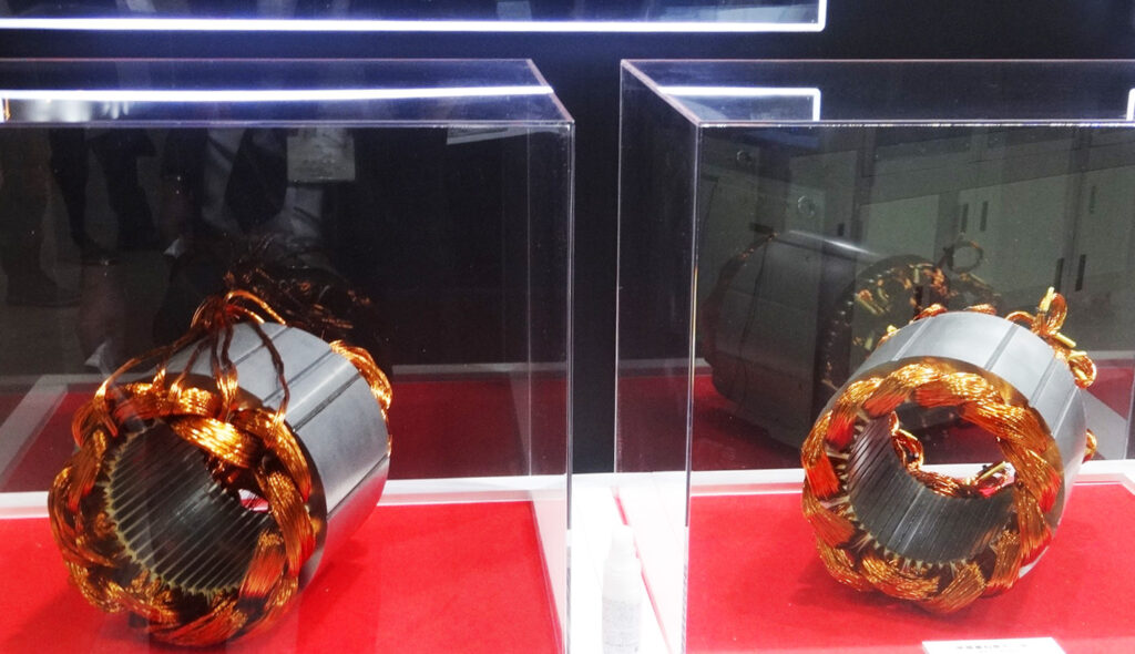
Panasonic Connect Co., Ltd. enters the blue laser processing machine market. The company will start receiving orders for a laser processing machine that adopts its original blue direct diode laser (DDL) in the first half of FY2023.
Additive Manufacturing
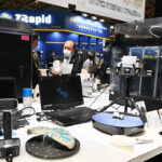
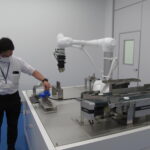
More and more three-dimensional (3D) printers are used at manufacturing sites. Today’s home electric appliances employ 3D printers that laminate resin. More recently, 3D printers that use metals are attracting attention. Also, the number of companies entering this field are increasing.
The metal method is classified into the powder method and the wire method. In the powder method, the metal powder is spread over on a flat surface and each layer is molten and solidified, and then laminated. Meanwhile, in the wire method, the wire for welding is molten to form high-quality 3D structure. The powder method forms complex and highly accurate shapes.
In 2019, Mitsubishi Electric Corporation entered the market and released a powder-based 3D printer. In 2022, it again released a wire-based 3D printer. The company targets to market the product for industrial application, including the manufacture of metal components for medical equipment, automobiles, and energy-related products.
Metal Bonding Technologies
Mainly, bonding technologies for metals used in the manufacturing process of electronic equipment are being diversified. These technologies include diffusion bonding; resistance welding, which applies the principle that heat is generated when electric current flows in a metal; laser welding, which uses heat generation by condensation of laser light; and ultrasonic bonding, in which metals are bonded by heat generated by vibrations occurring through the application of ultrasonic waves to metals.
Specifically, diffusion bonding technology bonds metals using the movement (diffusion) of atoms. Diffusion occurs by heating and applying pressure using melting point temperature or lower in a vacuum. The technology does not use adhesives. Also, it does not involve the melting of materials either. It features higher bonding strength and superior heat resistance compared with thermocompression bonding and brazing.
Tokyo-based Alone Co., Ltd. puts in place an integrated production system from design to production of fine metal components. It involves application of etching and diffusion bonding. Also, it applies etching stainless steel to make metal components. This technology etches stainless steel with a thickness of 50μm into a mesh, such as circle and triangle, and laminates 2020 meshes.
As carbon fiber reinforced plastics (CFRP) replace metals to reduce the weight of EVs, interests in bonding technology increases. In solder bonding, flux removes oxide film on the surface of metals. Likewise, surface reforming improves the bonding performance of resin.
FUJI Corporation enhances the bonding performance of metals through surface reforming using the property of electrically neutral radical in plasma. The company cultivates demand for its Tough Plasma atmospheric-pressure plasma unit. Frame processing involves a risk due to heat. However, FUJI’s atmospheric-pressure plasma unit uses low temperature irradiation gas. It removes organic contamination from metals and glass, as well as from rubber and resin that are weak to heat without causing deterioration of materials. It also achieves surface reforming, and improves functionalities and bonding strength of materials.
Press-Fit Mounting Method
Meanwhile, press-fit method mounts modules and dual inline package (DIP) components (lead components) such as connectors on printed circuit boards (PCBs) without using solder. The use of this method advances. Specifically, press-fit is a mounting technique that provides electrical connection and mechanical retention at the same time. It press-fits connectors’ terminals with spring property into through holes of PCBs. Thus, the technique eliminates the need for soldering.
Recently, the press-fit technique attracts attention as it can suppress equipment cost, such as reflow ovens, compared with soldering.
Mitsubishi Electric and Fuji Electric Co., Ltd. have been increasing promotion of insulated gate bipolar transistor (IGBT) modules that allow press-fit mounting when they produce power semiconductors.
- Share: