ASIA ELECTRONICS INDUSTRYYOUR WINDOW TO SMART MANUFACTURING
Ansys Solutions Get Certified for UMC's 3D Chip Technology
Ansys multiphysics solutions have been certified by global semiconductor foundry United Microelectronics Corp. (UMC) to simulate its latest 3D-IC WoW stacked technology. Mainly, this technology will improve the power, efficiency, and performance of edge AI, graphic processing, and wireless communication systems. Moreover, the certification empowers more chip designers to employ Ansys’ semiconductor simulation solutions that perform multi-die co-analysis for streamlining and ensuring successful design.
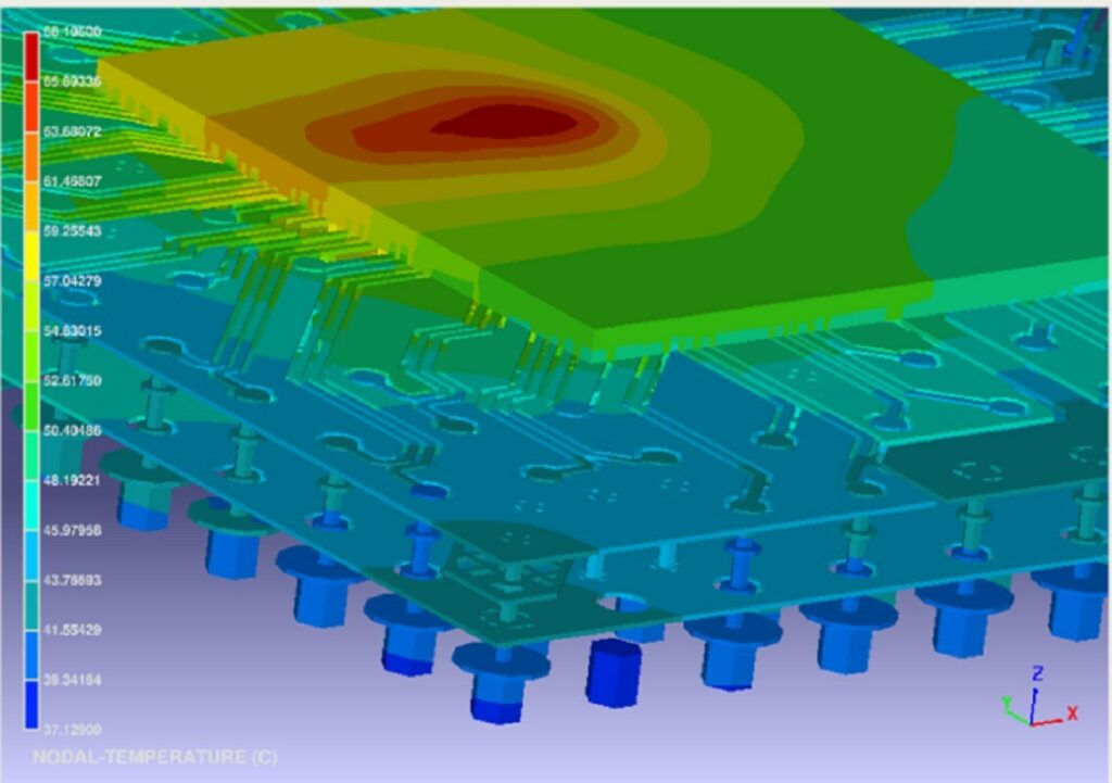
Specifically, WoW technology consists of silicon wafers, or dies vertically stacked rather than placed horizontally across a board. Built on cloud-optimized infrastructure, Ansys RedHawk-SC™ and Ansys RedHawk-SC Electrothermal™ have the speed, capacity, and predictive accuracy to handle full-chip analysis. These include multi-die packages and interconnects for power and signal integrity, thermal profiling, and more. Also, these 3D-IC solutions for multiphysics analysis fit into a larger set of comprehensive Ansys solutions for board and system electrothermal analysis, including Ansys SIwave™ and Ansys Icepak™.
“We’re pleased with the result of our collaboration with Ansys in the delivery of UMC technology reference flow. Specifically, it empowers customers to address growing performance, reliability, and power demands for cloud and data center applications,” said Osbert Cheng, vice president of device technology development and design support at UMC.
“The collaborative efforts combining Ansys’ comprehensive chip-package co-analysis solutions with UMC’s advanced chip-stacking technology address complex multiphysics challenges in 3D-IC packaging technologies,” continued Cheng.
“Ansys and UMC’s 3D-IC solutions address complex multiphysics challenges to meet stringent power, performance, thermal and reliability requirements,” said John Lee, vice president and general manager of the electronics, semiconductor, and optics business unit at Ansys. “Ansys’ dual-approach with both chip- and system-aware design solutions enable mutual customers to accelerate design convergence with greater confidence from small, delicate details at chip level to system-level design challenges.”
