ASIA ELECTRONICS INDUSTRYYOUR WINDOW TO SMART MANUFACTURING
PMT Offers 6-Inch Wafer Package Prototyping Service
Japanese foundry service provider, PMT Corporation has started prototyping service for 6-inch wafers in its foundry package business. Also, the company has successfully increased the wafer size through collaboration with Maxell, Ltd.
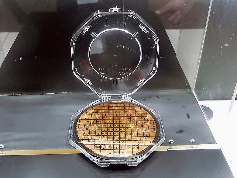
The company provides foundry services for wafer package prototypes, specializing in developing and prototyping rewiring packages. Since 2019, the company has been providing prototype services for fan-out wafer-level packaging (FOWLP) and wafer-level CSP (WLCSP) using 0.5-inch wafers made in a minimal fab. Since then, it was able to increase the wafer diameter to 1 inch. Successively, many prototypes have been produced for various applications.
Collaboration for Business Expansion
Specifically, the company began a collaboration with Maxell Ltd., Kyushu Works (Fukuoka Prefecture) in April 2022. This aims to expand the company’s package foundry business. In May 2022, it relocated the fab from the PMT head office factory in Kasuya, Fukuoka to the Kyushu office of Maxell. Primarily, this move aims to increase the wafer diameter to 6-inch.
Moreover, the company utilized the 6-inch fab for solder balls in the factory, thus increasing the wafer diameter. Then, it started to offer in September prototyping services for semiconductor packages using 6-inch wafers.
- Share: